ZHCS794B February 2012 – August 2015 SN75DP126
PRODUCTION DATA.
- 1 特性
- 2 应用
- 3 说明
- 4 修订历史记录
- 5 说明 (续)
- 6 Pin Configuration and Functions
-
7 Specifications
- 7.1 Absolute Maximum Ratings
- 7.2 ESD Ratings
- 7.3 Recommended Operating Conditions
- 7.4 Thermal Information
- 7.5 Power Supply Electrical Characteristics
- 7.6 Main Link Input Electrical Characteristics
- 7.7 DisplayPort Main Link Output Electrical Characteristics
- 7.8 HDMI/DVI Main Link Output Electrical Characteristics
- 7.9 HPD/CAD/EN Electrical Characteristics
- 7.10 AUX/DDC/I2C Electrical Characteristics
- 7.11 DisplayPort Main Link Output Switching Characteristics
- 7.12 HDMI/DVI Main Link Switching Characteristics
- 7.13 HPD/CAD Switching Characteristics
- 7.14 AUX/DDC/I2C Switching Characteristics
- 7.15 Typical Characteristics
-
8 Detailed Description
- 8.1 Overview
- 8.2 Functional Block Diagram
- 8.3
Feature Description
- 8.3.1 Implementing the EN Signal
- 8.3.2 Hot Plug Detect (HPD) and Cable Adapter Detect (CAD) Description
- 8.3.3 OVS Function Description
- 8.3.4 AUX and DDC Configuration Details
- 8.3.5 Source-Side Main Link EQ Configuration Details
- 8.3.6 DP-HDMI Adaptor ID Buffer
- 8.3.7 GPU with a Unified AUX/DDC Configuration
- 8.3.8 GPU with Separate DDC and AUX Channels
- 8.4 Device Functional Modes
- 8.5 Register Maps
- 9 Application and Implementation
- 10Power Supply Recommendations
- 11Layout
- 12器件和文档支持
- 13机械、封装和可订购信息
11 Layout
11.1 Layout Guidelines
- Decoupling with small current loops is recommended.
- It is recommended to place the de-coupling cap as close as possible to the device and on the same side of the PCB.
- Choose the capacitor such that the resonant frequency of the capacitor does not align closely with 5.4 GHz.
- Also provide several GND vias to the thermal pad to minimize the area of current loops.
11.1.1 Layer Stack
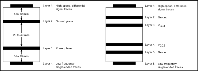 Figure 36. Recommended 4- or 6- Layer (0.062") Stack for a Receiver PCB Design
Routing the high-speed differential signal traces on the top layer avoids the use of vias (and the introduction of their inductances) and allows for clean interconnects from the DisplayPort connectors to the repeater inputs and from the repeater output to the subsequent receiver circuit.
Placing a solid ground plane next to the high-speed signal layer establishes controlled impedance for transmission line interconnects and provides an excellent low-inductance path for the return current flow.
Placing the power plane next to the ground plane creates additional high-frequency bypass capacitance.
Routing the fast-edged control signals on the bottom layer by prevents them from cross-talking into the high-speed signal traces and minimizes EMI.
If the receiver requires a supply voltage different from the one of the repeater, add a second power/ground plane system to the stack to keep it symmetrical. This makes the stack mechanically stable and prevents it from warping. Also, the power and ground plane of each power system can be placed closer together, thus increasing the high-frequency bypass capacitance significantly. Finally, a second power/ground system provides added isolation between the signal layers.
11.1.2 Power Plane Do's and Don'ts for Four-Layer Boards
Rreducing noise in four-layer board configurations is of paramount concern. The following guidelines should maintain the advantages gained in the four-layer board layout.
- Pay utmost attention to how the holes and cutouts in the planes are done. They break up the plane and, therefore, cause increased loop areas (see A and B in Figure 37).
- Avoid buried traces in the ground plane. If you have to use them, put them in the +V plane.
- When making through holes for 100-mil-center-spacing leads in the plane, place a small trace between each pin. Breaking up the plane with a row of holes is much better than having a long slot (see C and D in Figure 37).
- When splitting up the ground plane to make a digital and power ground for example, make sure that the signals connected to the microcomputer are still located entirely over the digital ground. Extending signal traces beyond the power ground is detrimental because the power ground does not work to reduce the loop area for digital noise signals.
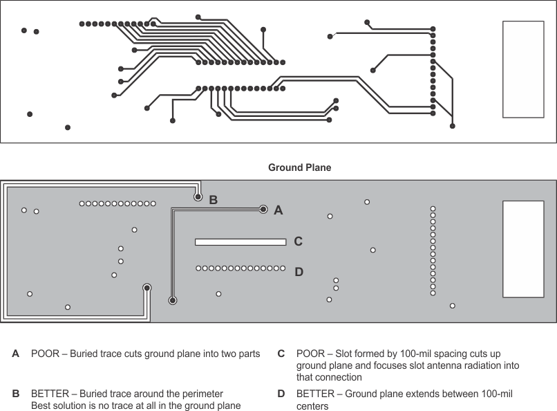 Figure 37. Four-Layer Board Layout Considerations
11.1.3 Differential Traces
Guidelines for routing PCB traces are necessary when trying to maintain signal integrity and lower EMI. Although there seems to be an endless number of precautions to be taken, this section provides only a few main recommendations as layout guidance.
- Reduce intra-pair skew in a differential trace by introducing small meandering corrections at the point of mismatch.
- Reduce inter-pair skew, caused by component placement and IC pinouts, by making larger meandering correction along the signal path. Use chamfered corners with a length-to-trace width ratio of between 3 and 5. The distance between bends should be 8 to 10 times the trace width.
- Use 45 degree bends (chamfered corners), instead of right-angle (90°) bends. Right-angle bends increase the effective trace width, which changes the differential trace impedance creating large discontinuities. A 45o bends is seen as a smaller discontinuity.
- When routing around an object, route both trace of a pair in parallel. Splitting the traces changes the line-to-line spacing, thus causing the differential impedance to change and discontinuities to occur.
- Place passive components within the signal path, such as source-matching resistors or ac-coupling capacitors, next to each other. Routing as in case a) creates wider trace spacing than in b), the resulting discontinuity, however, is limited to a far narrower area.
- When routing traces next to a via or between an array of vias, make sure that the via clearance section does not interrupt the path of the return current on the ground plane below.
- Avoid metal layers and traces underneath or between the pads off the DisplayPort connectors for better impedance matching. Otherwise they will cause the differential impedance to drop below 75 Ω and fail the board during TDR testing.
- Use the smallest size possible for signal trace vias and DisplayPort connector pads as they have less impact on the 100 Ω differential impedance. Large vias and pads can cause the impedance to drop below 85 Ω.
- Use solid power and ground planes for 100 Ω impedance control and minimum power noise.
- For 100 Ω differential impedance, use the smallest trace spacing possible, which is usually specified by the PCB vendor.
- Keep the trace length between the DisplayPort connector and the DisplayPort device as short as possible to minimize attenuation.
- Use good DisplayPort connectors whose impedances meet the specifications.
- Place bulk capacitors (for example, 10 μF) close to power sources, such as voltage regulators or where the power is supplied to the PCB.
- Place smaller 0.1 μF or 0.01 μF capacitors at the device.
11.2 Layout Example
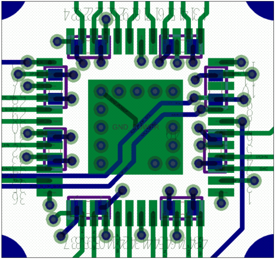 Figure 38. Thermal PAD Grounding
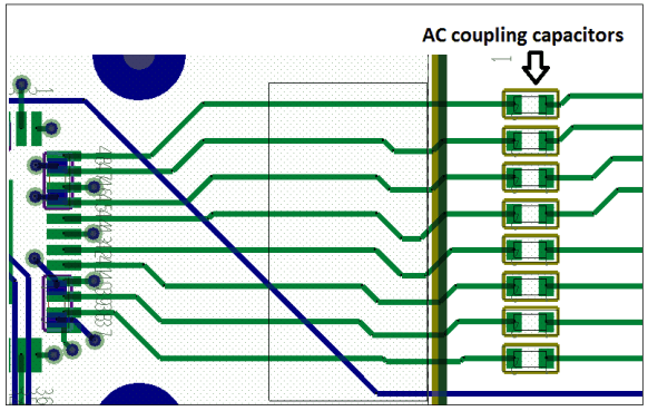 Figure 39. AC Capacitors Placement and Routing Example
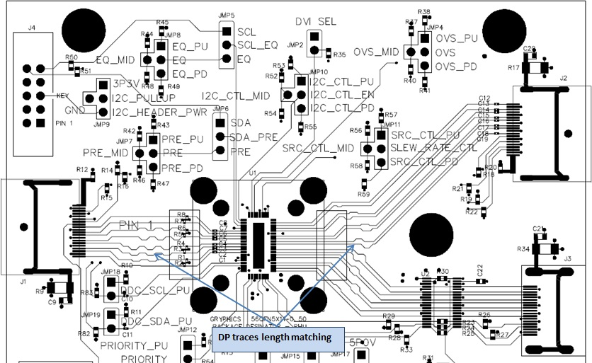 Figure 40. SN75DP126 Layout