SLLS009E October 1985 – March 2024 SN75ALS194
PRODUCTION DATA
- 1
- 1 Features
- 2 Applications
- 3 Description
- 4 Pin Configuration and Functions
- 5 Specifications
- 6 Parameter Measurement Information
- 7 Detailed Description
- 8 Device and Documentation Support
- 9 Revision History
- 10Mechanical, Packaging, and Orderable Information
封装选项
请参考 PDF 数据表获取器件具体的封装图。
机械数据 (封装 | 引脚)
- NS|16
- N|16
- D|16
散热焊盘机械数据 (封装 | 引脚)
- D|16
订购信息
5.7 Typical Characteristics
Data for temperatures below 0°C and above 70°C are applicable to the SN55ALS194 circuits only.
The A input is connected to VCC during the testing of the Y outputs and to GND during the testing of the Z outputs.
The A input is connected to ground during the testing of the Y outputs and to VCC during the testing of the Z outputs.
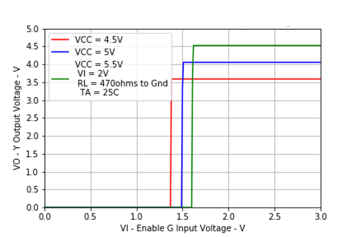 Figure 5-2 Y Output Voltage vs Data Input Voltage
 Figure 5-4 Y Output Voltage vs Enable G Input Voltage
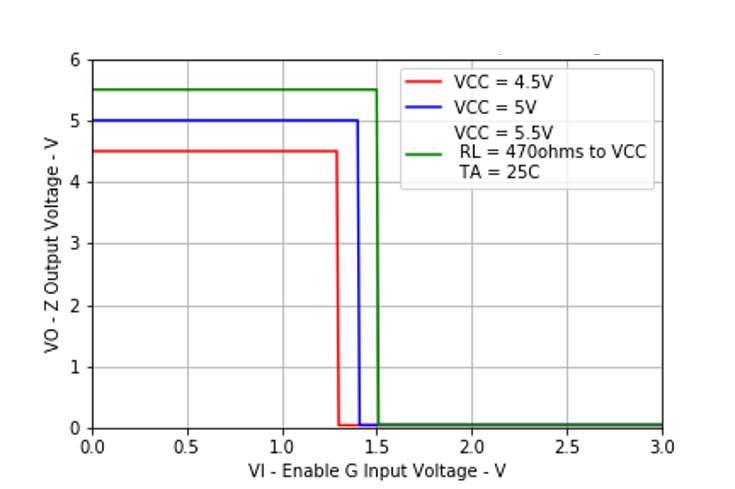 Figure 5-6 Z Output Voltage vs Enable G Input Voltage
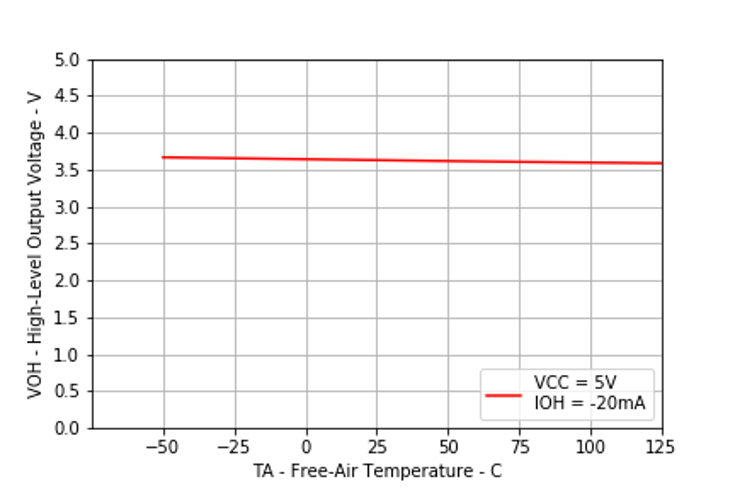 Figure 5-8 High-level Output Voltage vs Free-air Temperature
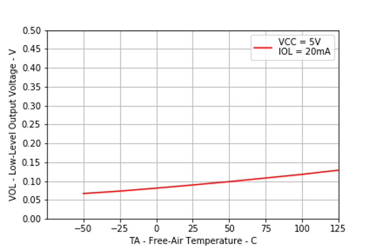 Figure 5-10 Low-level Output Voltage vs Free-air Temperature
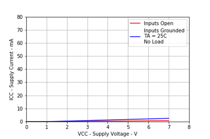 Figure 5-12 Supply Current vs Supply Voltage
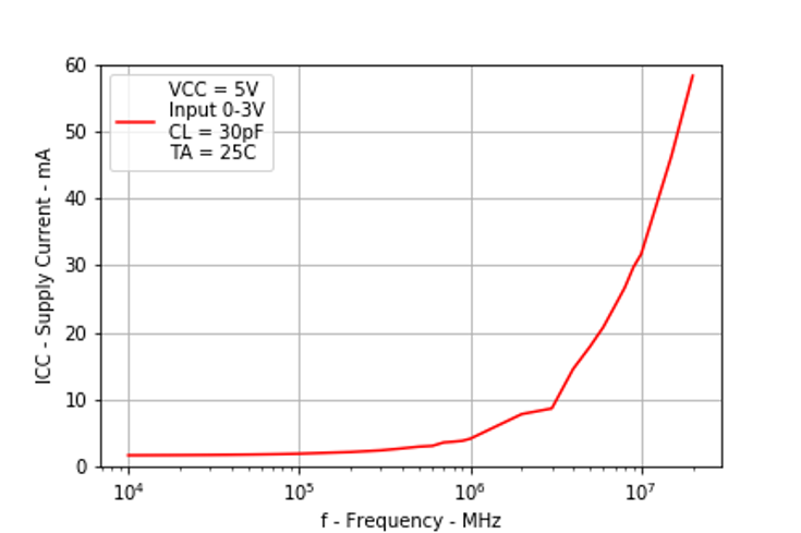 Figure 5-14 Supply Current vs Frequency
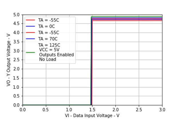 Figure 5-3 Y Output Voltage vs Data Input Voltage
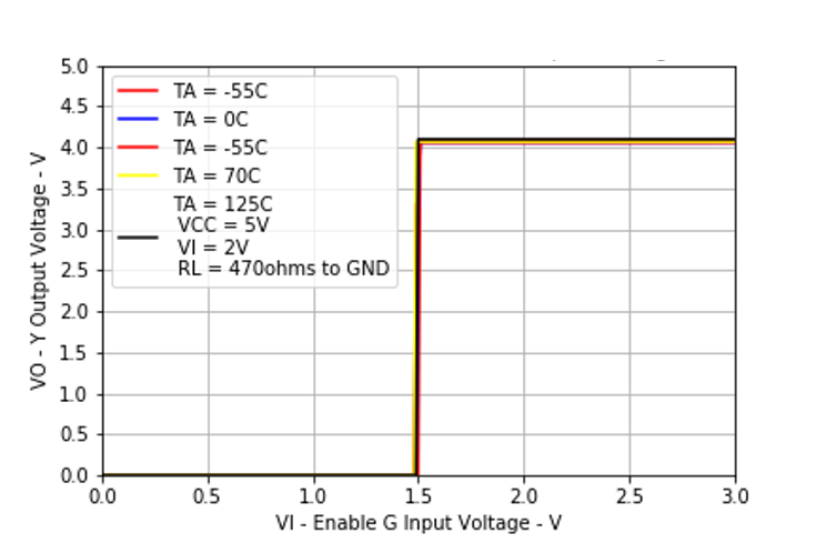 Figure 5-5 Y Output Voltage vs Enable G Input Voltage
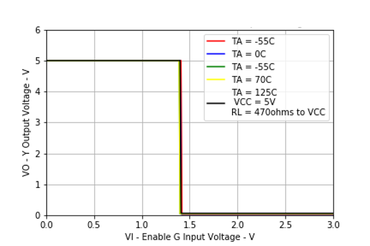 Figure 5-7 Z Output Voltage vs Enable G Input Voltage
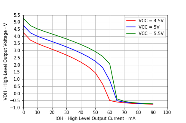 Figure 5-9 High-level Output Voltage vs High-level Output Current
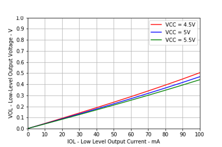 Figure 5-11 Low-level Output Voltage vs Low-level Output Current
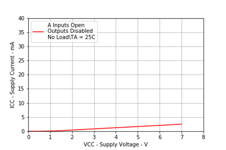 Figure 5-13 Supply Current vs Supply Voltage