SLLS009E October 1985 – March 2024 SN75ALS194
PRODUCTION DATA
- 1
- 1 Features
- 2 Applications
- 3 Description
- 4 Pin Configuration and Functions
- 5 Specifications
- 6 Parameter Measurement Information
- 7 Detailed Description
- 8 Device and Documentation Support
- 9 Revision History
- 10Mechanical, Packaging, and Orderable Information
封装选项
请参考 PDF 数据表获取器件具体的封装图。
机械数据 (封装 | 引脚)
- NS|16
- N|16
- D|16
散热焊盘机械数据 (封装 | 引脚)
- D|16
订购信息
3 Description
These four differential line drivers are designed for data transmission over twisted-pair or parallel-wire transmission lines. They meet the requirements of ANSI Standard EIA/TIA-422-B and ITU Recommendation V.11 and are compatible with 3-state TTL circuits. Advanced low-power Schottky technology provides high speed without the usual power penalty. Standby supply current is typically only 26mA. Typical propagation delay time is less than 10ns, and enable/disable times are typically less than 16ns.
High-impedance inputs keep input currents low: less than 1µA for a high level and less than 100µA for a low level. The driver circuits can be enabled in pairs by separate active-high enable inputs. The SN75ALS194 is capable of data rates in excess of 20 megabits per second and is designed to operates with the SN75ALS195 quadruple line receiver.
The SN75ALS194 is characterized for operation from 0°C to 70°C.
| PART NUMBER | PACKAGE(1) | PACKAGE SIZE(2) |
|---|---|---|
| SN75ALS194 | NS (SOP, 16) | 10.2mm × 7.8mm |
| D (SOIC, 16) | 9.9mm × 6mm | |
| N (PDIP, 16) | 19.3mm × 9.4mm |
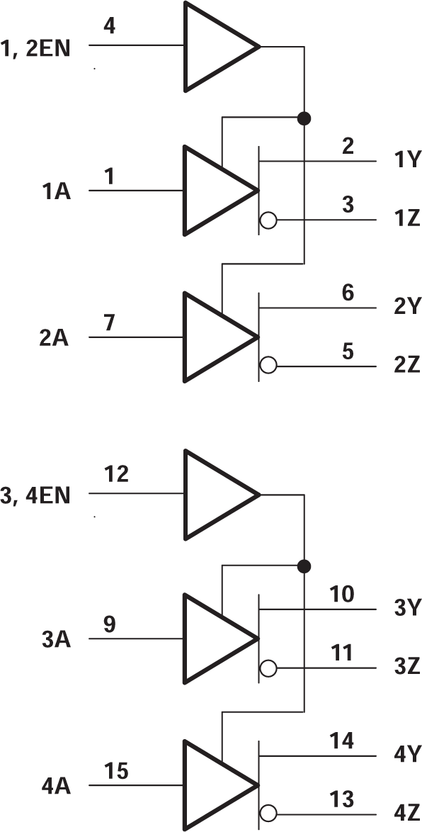
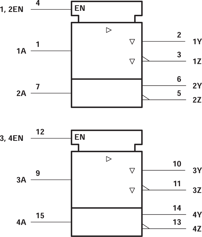
 Logic Diagram (Positive
Logic)