SLLS009E October 1985 – March 2024 SN75ALS194
PRODUCTION DATA
- 1
- 1 Features
- 2 Applications
- 3 Description
- 4 Pin Configuration and Functions
- 5 Specifications
- 6 Parameter Measurement Information
- 7 Detailed Description
- 8 Device and Documentation Support
- 9 Revision History
- 10Mechanical, Packaging, and Orderable Information
封装选项
请参考 PDF 数据表获取器件具体的封装图。
机械数据 (封装 | 引脚)
- NS|16
- N|16
- D|16
散热焊盘机械数据 (封装 | 引脚)
- D|16
订购信息
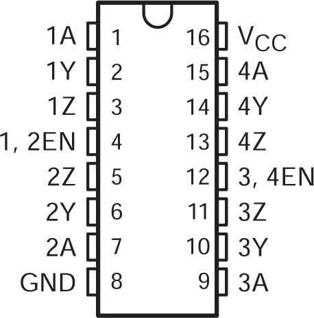
4 Pin Configuration and Functions
 Figure 4-1 D, N, or NS Package
(Top View)
Table 4-1 Pin Functions
| PIN | TYPE(1) | DESCRIPTION | |
|---|---|---|---|
| NAME | NO. | ||
| 1A | 1 | I | Single Ended Data Input for Channel 1 |
| 1Y | 2 | O | Non-Inverting Output for Differential Driver on Channel 1 |
| 1Z | 3 | O | Inverting Output of Differential Driver on Channel 1 |
| 1, 2EN | 4 | I | Channel 1 and 2 Enable |
| 2Z | 5 | O | Inverting Output of Differential Driver on Channel 2 |
| 2Y | 6 | O | Non-Inverting Output for Differential Driver on Channel 2 |
| 2A | 7 | I | Single Ended Data Input for Channel 2 |
| GND | 8 | GND | Device GND |
| 3A | 9 | I | Single Ended Data Input for Channel 3 |
| 3Y | 10 | O | Non-Inverting Output for Differential Driver on Channel 3 |
| 3Z | 11 | O | Inverting Output of Differential Driver on Channel 3 |
| 3, 4EN | 12 | I | Channel 3 and 4 Enable |
| 4Z | 13 | O | Inverting Output of Differential Driver on Channel 4 |
| 4Y | 14 | O | Non-Inverting Output for Differential Driver on Channel 4 |
| 4A | 15 | I | Single Ended Data Input for Channel 4 |
| VCC | 16 | PWR | Device VCC (4.75V to 5.25V) |
(1) Signal Types: I = Input, O = Output, I/O = Input or Output.