SCLS429K MAY 1999 – November 2016 SN74LV4052A
UNLESS OTHERWISE NOTED, this document contains PRODUCTION DATA.
- 1 Features
- 2 Applications
- 3 Description
- 4 Revision History
- 5 Pin Configuration and Functions
-
6 Specifications
- 6.1 Absolute Maximum Ratings
- 6.2 ESD Ratings
- 6.3 Recommended Operating Conditions
- 6.4 Thermal Information
- 6.5 Electrical Characteristics
- 6.6 Switching Characteristics: VCC = 2.5 V ± 0.2 V
- 6.7 Switching Characteristics: VCC = 3.3 V ± 0.3 V
- 6.8 Switching Characteristics: VCC = 5 V ± 0.5 V
- 6.9 Switching Characteristics: Analog
- 6.10 Operating Characteristics
- 6.11 Typical Characteristics
- 7 Parameter Measurement Information
- 8 Detailed Description
- 9 Application and Implementation
- 10Power Supply Recommendations
- 11Layout
- 12Device and Documentation Support
- 13Mechanical, Packaging, and Orderable Information
封装选项
请参考 PDF 数据表获取器件具体的封装图。
机械数据 (封装 | 引脚)
- DB|16
- PW|16
- NS|16
- RGY|16
- N|16
- D|16
- DGV|16
散热焊盘机械数据 (封装 | 引脚)
- RGY|16
订购信息
9 Application and Implementation
NOTE
Information in the following applications sections is not part of the TI component specification, and TI does not warrant its accuracy or completeness. TI’s customers are responsible for determining suitability of components for their purposes. Customers should validate and test their design implementation to confirm system functionality.
9.1 Application Information
Typical applications for the SN74LV4052A include signal gating, chopping, modulation or demodulation (modem), and signal multiplexing for analog-to-digital and digital-to-analog conversion systems.
9.2 Typical Application
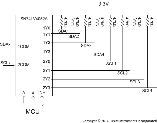
 Figure 13. Typical I2C Multiplexing Application
9.2.1 Design Requirements
Designing with the SN74LV4052A device requires a stable input voltage between 2 V and 5.5 V (see Recommended Operating Conditions for details). Another important design consideration are the characteristics of the signal being multiplexed which ensures no important information is lost due to timing or incompatibility with this device.
9.2.2 Detailed Design Procedure
The SN74LV4052A dual 1- to 4-channel multiplexer is ideal for I2C selection. The I2C data and clock lines are selected using A,B select lines from the MCU. The pullup resistors are selected based on the capability of the driver. Low pullup resistor results in faster rise time; however, it generates additional current during the low state into the driver. See to the Recommended Operating Conditions of the datasheet for the input transition rates (VIH and VIL) of the CMOS inputs.
9.2.3 Application Curve
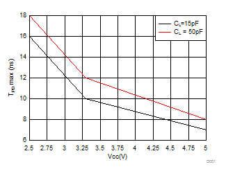
 Figure 14. Maximum Propagation Delay vs Vcc