SCLS469F March 2003 – December 2014 SN74LV4052A-Q1
PRODUCTION DATA.
- 1 Features
- 2 Applications
- 3 Description
- 4 Revision History
- 5 Pin Configuration and Functions
- 6 Specifications
- 7 Parameter Measurement Information
- 8 Detailed Description
- 9 Application and Implementation
- 10Power Supply Recommendations
- 11Layout
- 12Device and Documentation Support
- 13Mechanical, Packaging, and Orderable Information
封装选项
机械数据 (封装 | 引脚)
散热焊盘机械数据 (封装 | 引脚)
- D|16
订购信息
11 Layout
11.1 Layout Guidelines
In general, it is best to keep signal lines as short and as straight as possible. Incorporation of microstrip or stripline techniques is also recommended when signal lines are greater than 1 inch in length. These traces must be designed with a characteristic impedance of either 50 Ω or 75 Ω,as required by the application. Be careful placing this device too close to high voltage switching components, as they may cause interference.
11.2 Layout Example
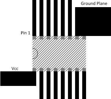 Figure 12. Layout Example Schematic