SCLS469F March 2003 – December 2014 SN74LV4052A-Q1
PRODUCTION DATA.
- 1 Features
- 2 Applications
- 3 Description
- 4 Revision History
- 5 Pin Configuration and Functions
- 6 Specifications
- 7 Parameter Measurement Information
- 8 Detailed Description
- 9 Application and Implementation
- 10Power Supply Recommendations
- 11Layout
- 12Device and Documentation Support
- 13Mechanical, Packaging, and Orderable Information
封装选项
机械数据 (封装 | 引脚)
散热焊盘机械数据 (封装 | 引脚)
- D|16
订购信息
8 Detailed Description
8.1 Overview
This device is a dual 4-channel analog multiplexer. A multiplexer is often used when several signals need to share the same device or resource. This device allows the selection of one of these signals at a time for analysis or propagation.
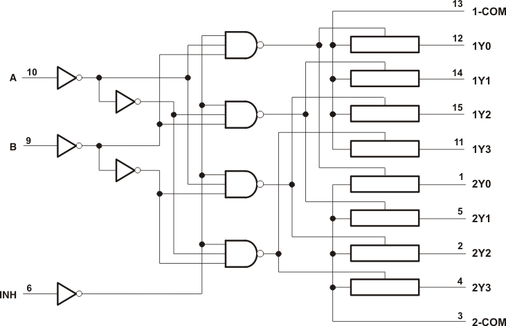
8.2 Functional Block Diagram
8.3 Feature Description
This device contains 2 separate 4-channel multiplexers for use in a variety of applications. The 4-channel multiplexers can also be configured as demultiplexers by using the COM pins as inputs and the 1Yx or 2Yx pins as outputs. This device is qualified for automotive applications and has an extended temperature range of -40C to 125C (maximum depends on package type).