ZHCSSG5L October 1995 – February 2024 SN54AHC08 , SN74AHC08
PRODUCTION DATA
- 1
- 1 特性
- 2 应用
- 3 说明
- 4 Pin Configuration and Functions
-
5 Specifications
- 5.1 Absolute Maximum Ratings
- 5.2 ESD Ratings
- 5.3 Recommended Operating Conditions
- 5.4 Thermal Information
- 5.5 Electrical Characteristics, TA = 25°C
- 5.6 Electrical Characteristics, TA = –55°C to 125°C
- 5.7 Electrical Characteristics, TA = –40°C to 125°C
- 5.8 Switching Characteristics, VCC = 3.3 V ± 0.3 V
- 5.9 Switching Characteristics, VCC = 5 V ± 0.5 V
- 5.10 Noise Characteristics
- 5.11 Operating Characteristics
- 5.12 Typical Characteristics
- 6 Parameter Measurement Information
- 7 Detailed Description
- 8 Application and Implementation
- 9 Device and Documentation Support
- 10Revision History
- 11Mechanical, Packaging, and Orderable Information
封装选项
请参考 PDF 数据表获取器件具体的封装图。
机械数据 (封装 | 引脚)
- D|14
- RGY|14
- DGV|14
- PW|14
- DB|14
- BQA|14
- N|14
- NS|14
散热焊盘机械数据 (封装 | 引脚)
订购信息
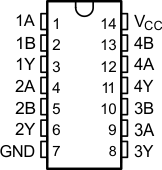
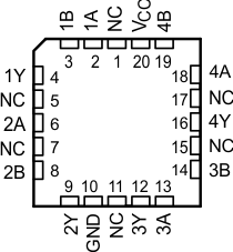
4 Pin Configuration and Functions
|
|
|
Figure 4-1 D, DB, DGV, N, NS, PW,
or W Package14-Pin SOIC, SSOP, TVSOP, PDIP, SO, or
TSSOP(Top
View)
|
Figure 4-2 FK Package20-Pin LCCC(Top View)
|
") Figure 4-3 RGY or BQA Package14-Pin VQFN or WQFN(Top View)
Figure 4-3 RGY or BQA Package14-Pin VQFN or WQFN(Top View)Table 4-1 Pin Functions
| PIN | I/O | DESCRIPTION | |||
|---|---|---|---|---|---|
| NAME | SOIC, SSOP, TVSOP, PDIP, SO, TSSOP | VQFN, WQFN | LCCC | ||
| 1A | 1 | 1 | 2 | I | 1A Input |
| 1B | 2 | 2 | 3 | I | 1B Input |
| 1Y | 3 | 3 | 4 | O | 1Y Output |
| 2A | 4 | 4 | 6 | I | 2A Input |
| 2B | 5 | 5 | 8 | I | 2B Input |
| 2Y | 6 | 6 | 9 | O | 2Y Output |
| 3Y | 8 | 8 | 12 | O | 3Y Output |
| 3A | 9 | 9 | 13 | I | 3A Input |
| 3B | 10 | 10 | 14 | I | 3B Input |
| 4Y | 11 | 11 | 16 | O | 4Y Output |
| 4A | 12 | 12 | 18 | I | 4A Input |
| 4B | 13 | 13 | 19 | I | 4B Input |
| GND | 7 | 7 | 10 | — | Ground Pin |
| NC | — | — | 1, 5, 7, 11, 15, 17 | — | No Connection |
| VCC | 14 | 14 | 20 | — | Power Pin |