SLOS073G March 1976 – November 2014 RC4558
PRODUCTION DATA.
- 1 Features
- 2 Applications
- 3 Description
- 4 Revision History
- 5 Pin Configuration and Functions
- 6 Specifications
- 7 Detailed Description
- 8 Application and Implementation
- 9 Power Supply Recommendations
- 10Layout
- 11Device and Documentation Support
- 12Mechanical, Packaging, and Orderable Information
封装选项
请参考 PDF 数据表获取器件具体的封装图。
机械数据 (封装 | 引脚)
- D|8
- P|8
- PS|8
- DGK|8
- PW|8
散热焊盘机械数据 (封装 | 引脚)
- PS|8
订购信息
10 Layout
10.1 Layout Guidelines
For best operational performance of the device, use good PCB layout practices, including:
- Noise can propagate into analog circuitry through the power pins of the circuit as a whole and the operational amplifier. Bypass capacitors are used to reduce the coupled noise by providing low impedance power sources local to the analog circuitry.
- Connect low-ESR, 0.1-μF ceramic bypass capacitors between each supply pin and ground, placed as close to the device as possible. A single bypass capacitor from V+ to ground is applicable for single supply applications.
- Separate grounding for analog and digital portions of circuitry is one of the simplest and most-effective methods of noise suppression. One or more layers on multilayer PCBs are usually devoted to ground planes. A ground plane helps distribute heat and reduces EMI noise pickup. Make sure to physically separate digital and analog grounds, paying attention to the flow of the ground current. For more detailed information, refer to Circuit Board Layout Techniques, (SLOA089).
- To reduce parasitic coupling, run the input traces as far away from the supply or output traces as possible. If it is not possible to keep them separate, it is much better to cross the sensitive trace perpendicular as opposed to in parallel with the noisy trace.
- Place the external components as close to the device as possible. Keeping RF and RG close to the inverting input minimizes parasitic capacitance, as shown in Layout Example.
- Keep the length of input traces as short as possible. Always remember that the input traces are the most sensitive part of the circuit.
- Consider a driven, low-impedance guard ring around the critical traces. A guard ring can significantly reduce leakage currents from nearby traces that are at different potentials.
10.2 Layout Example
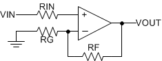 Figure 18. Operational Amplifier Schematic for Noninverting Configuration
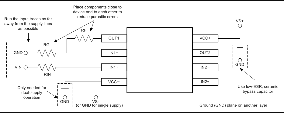 Figure 19. Operational Amplifier Board Layout for Noninverting Configuration