ZHCSL30B June 2009 – March 2020 PGA280
PRODUCTION DATA.
- 1 特性
- 2 应用
- 3 说明
- 4 修订历史记录
- 5 Pin Configuration and Functions
- 6 Specifications
-
7 Detailed Description
- 7.1 Overview
- 7.2 Functional Block Diagram
- 7.3 Feature Description
- 7.4 Device Functional Modes
- 7.5 Programming
- 7.6
Register Map
- 7.6.1 Register 0: Gain and External MUX Address (address = 00h) [reset = 0000 0000b]
- 7.6.2 Register 1: Software Reset Register (address = 01h) [reset = 0000 0000b]
- 7.6.3 Register 2: SPI: MODE Selection to GPIO-Pin (address = 02h) [reset = 0000 0000b]
- 7.6.4 Register 3: BUF Timeout Register (address = 03h) [reset = 0001 1001b]
- 7.6.5 Register 4: Error Register (address = 04h) [reset = 0000 0000b]
- 7.6.6 Register 5: GPIO Register (address = 05h) [reset = 0000 0000b]
- 7.6.7 Register 6: Input Switch Control Register 1 (address = 06h) [reset = 0110 0000b]
- 7.6.8 Register 7: Input Switch Control Register 2 (address =07h ) [reset = 0000 0000b]
- 7.6.9 Register 8: GPIO Configuration Register (address = 08h) [reset = 0000 0000b]
- 7.6.10 Register 9: CS Configuration Mode Register (address = 09h) [reset = 0000 0000b]
- 7.6.11 Register 10: Configuration Register 1 (address = 0Ah) [reset = 0000 0000b]
- 7.6.12 Register 11: Configuration Register 2 (address = 0Bh) [reset = 0001 0000b]
- 7.6.13 Register 12: Special Functions Register (address = 0Ch) [reset = 0000 0000b]
- 8 Application and Implementation
- 9 Power Supply Recommendations
- 10器件和文档支持
- 11机械、封装和可订购信息
7.3.1.9 Error Detection
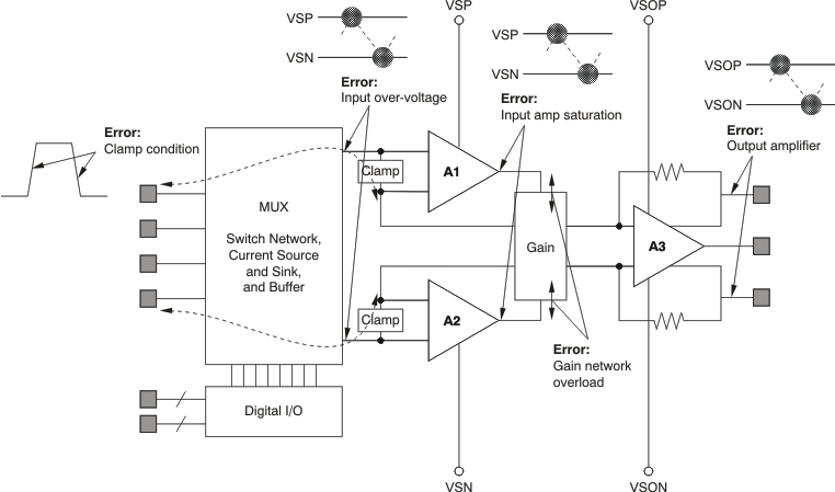
The PGA280 is designed for high dc precision and universal use, but the device also allows monitoring of signal integrity. The device contains an input switch network for signal tests and sense points that can indicate critical conditions. These added features support fully automated system setup and diagnostic capability. Out-of linear range conditions are detected and stored in the Error Status Register (Register 4) until reset. The input switches shown in Figure 44 can be used to short the input to GND, disconnect the signal, insert a 100µA test current, discharge external capacitance, and switch to a ground (VSON)-referenced signal measurement to observe the signal at the pin (versus the differential measurement). Figure 49 illustrates the diagnostic points available for error detection in the device architecture.
All switches are controlled through the SPI. The error signals can be combined using a logic OR function to an output pin and eventually be used as an error interrupt signal. Errors are normally latched, unless the LTD bit (latch disable) is set.
The error sensors are filtered with a suppression delay (Register 11). These error signals are normally suppressed during the buffer (BUFA) active time.

NOTE:
The signal path is observed for possible limitations; flags are stored and indicated in Register 4.