ZHCSL30B June 2009 – March 2020 PGA280
PRODUCTION DATA.
- 1 特性
- 2 应用
- 3 说明
- 4 修订历史记录
- 5 Pin Configuration and Functions
- 6 Specifications
-
7 Detailed Description
- 7.1 Overview
- 7.2 Functional Block Diagram
- 7.3 Feature Description
- 7.4 Device Functional Modes
- 7.5 Programming
- 7.6
Register Map
- 7.6.1 Register 0: Gain and External MUX Address (address = 00h) [reset = 0000 0000b]
- 7.6.2 Register 1: Software Reset Register (address = 01h) [reset = 0000 0000b]
- 7.6.3 Register 2: SPI: MODE Selection to GPIO-Pin (address = 02h) [reset = 0000 0000b]
- 7.6.4 Register 3: BUF Timeout Register (address = 03h) [reset = 0001 1001b]
- 7.6.5 Register 4: Error Register (address = 04h) [reset = 0000 0000b]
- 7.6.6 Register 5: GPIO Register (address = 05h) [reset = 0000 0000b]
- 7.6.7 Register 6: Input Switch Control Register 1 (address = 06h) [reset = 0110 0000b]
- 7.6.8 Register 7: Input Switch Control Register 2 (address =07h ) [reset = 0000 0000b]
- 7.6.9 Register 8: GPIO Configuration Register (address = 08h) [reset = 0000 0000b]
- 7.6.10 Register 9: CS Configuration Mode Register (address = 09h) [reset = 0000 0000b]
- 7.6.11 Register 10: Configuration Register 1 (address = 0Ah) [reset = 0000 0000b]
- 7.6.12 Register 11: Configuration Register 2 (address = 0Bh) [reset = 0001 0000b]
- 7.6.13 Register 12: Special Functions Register (address = 0Ch) [reset = 0000 0000b]
- 8 Application and Implementation
- 9 Power Supply Recommendations
- 10器件和文档支持
- 11机械、封装和可订购信息
7.4.1.1 CS Mode
A special CS mode for the GPIO extends the device communications to other external SPI devices, such as data converters or shift registers. This CS function is intended for SPI communication using four isolation couplers. To use this mode, follow this procedure:
Configure the desired GPIO pins as outputs in Register 8, then configure the respective ECS (extended CS) bits in Register 9.
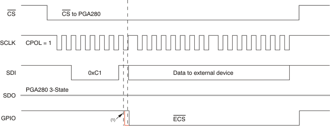
Register 2 allows control of the clock mode by CPn (n for the individual ECS pins). CP = 1 asserts ECS after the last negative SCLK edge of the command; CP = 0 asserts ECS after the positive SCLK, as Figure 50 shows.
Use the CS command 1100 0cccb [ccc = CS coded for 0 to 7] to activate ECS on a single GPIO pin.
Example for ECS on pin GPIO1 (CHKsum disabled):
0x4802 GPIO1 configured output (Note: GPIO may output a previously stored state; default is all zeroes)
0x4902 Assign CS (ECS) mode to GPIO1
0xC1 Single byte command to activate CS on GPIO1

This CS pin (ECS) stays low as long as CS to the PGA280 is held low. The PGA280 SDO is turned to a high-impedance output (and requires external termination). The PGA280 ignores both clock and data signals during this time. Therefore, data can be read and written to another device selected by the ECS port. Communication is terminated by setting CS (to the PGA280) to high; this toggle also sets the port ECS to high and terminates the I/O transfer with the other device.
Figure 50 shows the timing for the GPIO-generated ECS pulse in clock mode SPOL = 1 (SCLK is high after CS asserts low). Register 2 allows activating SPOL = 0 by writing a 1 to the CP bit, according to SPI mode1. The initial setting is SPOL = 1.
Mode1; set bit to 1: a positive edge of SCLK follows after ECS asserts low (CP = 0). See the red edge of the GPIO trace in Figure 50.
Mode2; set bit to 0: a negative edge of SCLK follows after ECS asserts high (CP = 1). See the black edge of the GPIO trace in Figure 50.
The negative edge of SCLK senses data. The positive edge of SCLK sets data on the data out line (if applicable).
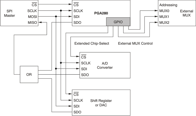
For SPI modes 0 or 3, SCLK must be inverted to indirectly sense data with the positive edge of SCLK. Figure 51 shows an example of connecting additional SPI devices, addressed by the ECS. The OR connection for SDO can be a wired-OR if all devices provide a 3-state output option with the respective device CS (ECS) set high.
The SPI interface allows clock rates higher than 10 MHz. Clock rates less than 10 MHz are recommended when using the ECS mode for less critical printed circuit board (PCB) layout and timing. Observe delays and distortion generated from isolation couplers. External drivers may be required to drive long and terminated cables.
With only four isolation couplers (digital galvanic isolation) connected in the SPI wires, the SPI can provide galvanic isolation for input and output channels. Figure 51 shows a block diagram of how to connect SPI devices selected by the ECS (extended CS) signal.
Isolation couples or long SPI cables in harsh industrial environment are sensitive to impairments. For improved communication integrity, the communication can be extended with a checksum byte.
Figure 51 shows an example of the GPIO pins used for both the extended chip select and special functions.
The chip select (CS) is connected to the PGA280 alone. The serial data input (SDI) and the serial clock (SCLK) are shared connections, and are connected to all devices [PGA280, A/D converter, and the shift register or digital-to-analog converter (DAC)]. The serial data output comes from each of the devices and are OR-connected or sent to an OR gate, to be received by the master. An OR gate is only required if the connected devices do not support 3-state operation. The PGA280 provides a 3-state output if not active. Pullup resistors may be required.
As mentioned previously, the GPIO pins are used to control an external multiplexer. In Figure 51, the three pins from GPIO0, GPIO1, and GPIO2 are used as a MUX address. Two other GPIO pins are used as ECS to enable communications with other slave devices.
 Figure 51. Example for Connecting Two Additional SPI Devices Selected by ECS