ZHCSNJ4B September   2007  – March 2021 PCA9543A

PRODUCTION DATA  

  1. 特性
  2. 应用
  3. 说明
  4. Revision History
  5. Pin Configuration and Functions
  6. Specifications
    1. 6.1 Absolute Maximum Ratings
    2. 6.2 ESD Ratings
    3. 6.3 Recommended Operating Conditions
    4. 6.4 Thermal Information
    5. 6.5 Electrical Characteristics
    6. 6.6 I2C Interface Timing Requirements
    7. 6.7 Switching Characteristics
    8. 6.8 Interrupt and Reset Timing Requirements
  7. Parameter Measurement Information
  8. Detailed Description
    1. 8.1 Overview
    2. 8.2 Functional Block Diagram
    3. 8.3 Feature Description
    4. 8.4 Device Functional Modes
      1. 8.4.1 RESET Input
      2. 8.4.2 Power-On Reset
    5. 8.5 Programming
      1. 8.5.1 I2C Interface
    6. 8.6 Control Register
      1. 8.6.1 Device Address
      2. 8.6.2 Control Register Description
      3. 8.6.3 Control Register Definition
      4. 8.6.4 Interrupt Handling
  9. Application and Implementation
    1. 9.1 Application Information
    2. 9.2 Typical Application
      1. 9.2.1 Design Requirements
      2. 9.2.2 Detailed Design Procedure
      3. 9.2.3 Application Curves
  10. 10Power Supply Recommendations
    1. 10.1 Power-On Reset Requirements
  11. 11Layout
    1. 11.1 Layout Guidelines
    2. 11.2 Layout Example
  12. 12Device and Documentation Support
    1. 12.1 Receiving Notification of Documentation Updates
    2. 12.2 Support Resources
    3. 12.3 Trademarks
    4. 12.4 Electrostatic Discharge Caution
    5. 12.5 Glossary
  13. 13Mechanical, Packaging, and Orderable Information

封装选项

机械数据 (封装 | 引脚)
散热焊盘机械数据 (封装 | 引脚)
订购信息

Detailed Design Procedure

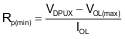
Once all the slaves are assigned to the appropriate slave channels and bus voltages are identified, the pull-up resistors, Rp, for each of the buses need to be selected appropriately. The minimum pull-up resistance is a function of VDPUX, VOL,(max), and IOL:

Equation 1. GUID-DF0F3A9C-156A-4A4C-8F5C-DCE73D2EBE64-low.gif

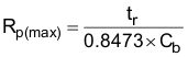
The maximum pull-up resistance is a function of the maximum rise time, tr (300 ns for fast-mode operation, fSCL = 400 kHz) and bus capacitance, Cb:

Equation 2. GUID-67D53CC3-D09D-45E4-A78E-72F00894BACE-low.gif

The maximum bus capacitance for an I2C bus must not exceed 400 pF for fast-mode operation. The bus capacitance can be approximated by adding the capacitance of the PCA9543A, Cio(OFF), the capacitance of wires/connections/traces, and the capacitance of each individual slave on a given channel. If both channels will be activated simultaneously, each of the slaves on both channels will contribute to total bus capacitance.