ZHCSII6C July 2018 – January 2023 OPA855
PRODUCTION DATA
- 1 特性
- 2 应用
- 3 说明
- 4 Revision History
- 5 Device Comparison Table
- 6 Pin Configuration and Functions
- 7 Specifications
- 8 Parameter Measurement Information
- 9 Detailed Description
- 10Application, Implementation, and Layout
- 11Device and Documentation Support
- 12Mechanical, Packaging, and Orderable Information
10.3 Typical Application
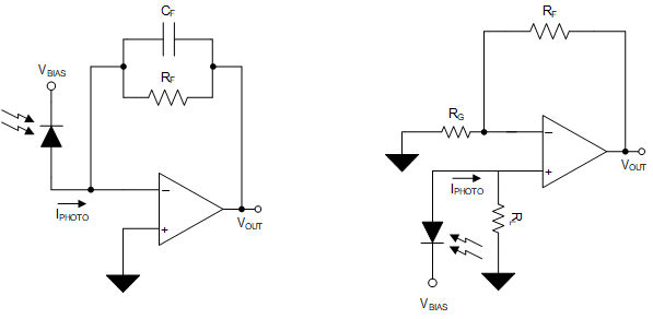
There are two main approaches for current to voltage conversion. One uses a non-inverting voltage feedback amplifier in combination with a shunt resistor to first convert current and then further amplify the optical signal. The other approach configures an amplifier for transimpedance applications which combines both steps into one. Figure 10-4 shows the standard configuration for both approaches.
 Figure 10-4 Transimpedance Amplifier vs. Voltage Feedback Amplifier
Both configurations provide a low output impedance stage which provides the ability to interface with various types of loads. However, the non-inverting option comes with a few disadvantages. TIA's input impedance is near zero, since the amplifier keeps the voltage at the inverting input node at the same potential as the non-inverting input node. While the VFB's input impedance is equal to the shunt resistor RL. In the case of the VFB amplifier, the signal response will be slowed due to a large time constant created by the shunt resistor and capacitor. Also, the linearity of the photodetector can suffer, especially for higher detector currents due to the varying voltage bias produced at the shunt resistor. And, since the voltage bias of the photodetector is no longer constant for all detector currents, the diode’s internal capacitance will vary. Using a TIA, the voltage bias remains constant at the voltage set by the non-inverting node, and can provide level shifting to the signal which is especially useful for single-supply configurations.
OPA855 offers 8 GHz of gain bandwidth, high slew-rate, and low noise which makes this device suitable for a wide range of photodetectors. Figure 10-5 shows the OPA855 configured as a transimpedance amplifier (TIA) in a wide-bandwidth, optical front-end system. Various types of optical sensors can be used as an optical input to the amplifier: photodiode (PD), avalanche photodiode (APD), Photomultiplier Tube (PMT), and Multi-Pixel Photon Counter (MPPC) or known as Solid-State Photomultiplier (SiPM). Optical detection applications have commonly used APDs, but ultra-low light source detection has been a challenge in past solutions. With technologies such as PMTs and MPPCs, their high intrinsic gain, while maintaining a fast output, requires a low noise, high-speed interface. The OPA855 can accommodate for these optical challenges and would work equally as well in these applications.
 Figure 10-5 Transimpedance Amplifier with APD or SiPM/MPPC or PMT Inputs
Transimpedance applications require low voltage and current noise for optimal system performance. Due to its high input impedance structure, the OPA855 has a great balance between low input-referred voltage noise and current noise which is consistent over frequency. Overall, the amplifier noise should have minimal impact to the total noise of the application. We would need to examine the total input referred noise to the optical sensor.
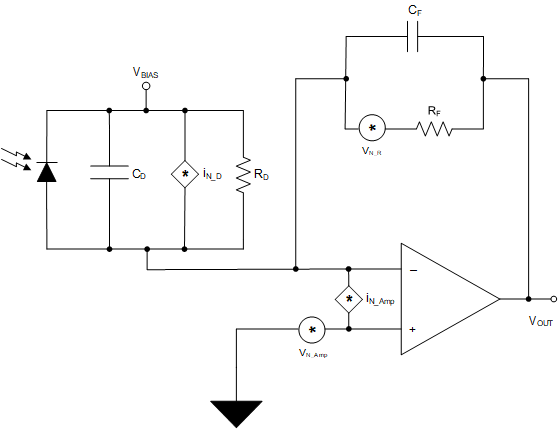
Noise sources in optical sensors vary especially when introducing gain and photon paralleling. Optical power, gain, and applied reverse bias are the main characteristics that will affect signal to noise ratio. Standard photodiodes contribute the lowest noise at the highest quantum efficiency. Internal to photodiodes, noises sources include shot and thermal. Shot noise is a random occurrence of photodetection which arises in periods of both light and dark. Dark current is noise that occurs in the absence of an optical source which can be included with shot noise. And, thermal noise originates from the shunt resistance internal to the diode. At the lower signal levels, shot noise will dominate. Figure 10-6 shows an example of the noise sources present in a transimpedance amplifier circuit. The total TIA noise is the root sum square of each component within the system: photodiode noise, amplifier current noise, amplifier voltage noise, and feedback resistor noise.
 Figure 10-6 Photodiode and TIA Noise Model
Interfacing with APDs is similar to interfacing with PIN PDs, but APDs have additional noise factors due to its internal gain. APDs have increased shot noise and the addition of a multiplication excess noise factor. Decreasing capacitance, increasing diode shunt resistance, and decreasing reverse voltage bias applied to the APD deceases noise at the expense of response time. MPPCs' total noise is comparable to APDs, but with differing noise sources. This optical sensor includes digital-like noise factors such as dark count rate, after pulsing, and optical crosstalk due to its paralleling gain cells. For PMTs, dark count rate is lower. In general, PMTs’ total noise is comparable to PDs’ with an internal gain comparable to APDs'. However, PMTs have the lowest quantum efficiency of the optical sensor space.