ZHCSK40D August 2019 – July 2020 OPA810
PRODUCTION DATA
- 1 特性
- 2 应用
- 3 说明
- 4 Revision History
- 5 Device Comparison Table
- 6 Pin Configuration and Functions
-
7 Specifications
- 7.1 Absolute Maximum Ratings
- 7.2 ESD Ratings
- 7.3 Recommended Operating Conditions
- 7.4 Thermal Information
- 7.5 Electrical Characteristics: 10 V
- 7.6 Electrical Characteristics: 24 V
- 7.7 Electrical Characteristics: 5 V
- 7.8 Typical Characteristics: VS = 10 V
- 7.9 Typical Characteristics: VS = 24 V
- 7.10 Typical Characteristics: VS = 5 V
- 7.11 Typical Characteristics: ±2.375-V to ±12-V Split Supply
- 8 Detailed Description
- 9 Application and Implementation
- 10Power Supply Recommendations
- 11Layout
- 12Device and Documentation Support
封装选项
机械数据 (封装 | 引脚)
散热焊盘机械数据 (封装 | 引脚)
订购信息
9.1.3 Noise Analysis and the Effect of Resistor Elements on Total Noise
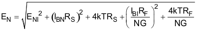
The OPA810 provides a low input-referred broadband noise voltage density of 6.3 nV/√ Hz while requiring a low 3.7-mA quiescent supply current. To take full advantage of this low input noise, careful attention to the other possible noise contributors is required. Figure 9-10 shows the operational amplifier noise analysis model with all the noise terms included. In this model, all the noise terms are taken to be noise voltage or current density terms in nV/√ Hz or pA/√ Hz.
 Figure 9-10 Operational Amplifier Noise Analysis Model
The total output spot noise voltage is computed as the square root of the squared contributing terms to the output noise voltage. This computation adds all the contributing noise powers at the output by superposition, then calculates the square root to get back to a spot noise voltage. Figure 9-10 shows the general form for this output noise voltage using the terms shown in Equation 7.
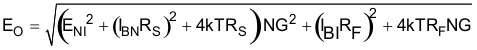
Dividing this expression by the noise gain (NG = 1 + RF / RG) shows the equivalent input referred spot noise voltage at the noninverting input; see Equation 8.
Substituting large resistor values into Equation 8 can quickly dominate the total equivalent input referred noise. A source impedance on the noninverting input of 2-kΩ adds a Johnson voltage noise term similar to that of the amplifier (6.3 nV/√ Hz).
Table 9-1 compares the noise contributions from the various terms when the OPA810 is configured in a noninverting gain of 5 V/V as Figure 9-11 shows. Two cases are considered where the resistor values in case 2 are 10x the resistor values in case 1. The total output noise in case 1 is 34 nV/√ Hz while the noise in case 2 is 51.5 nV/√ Hz. The large value resistors in case 2 dilute the benefits of selecting a low noise amplifier like the OPA810. To minimize total system noise, reduce the size of the resistor values. This increases the amplifiers output load and results in a degradation of distortion performance. The increased loading increases the dynamic power consumption of the amplifier. The circuit designer must make the appropriate tradeoffs to maximize the overall performance of the amplifier to match the system requirements.
 Figure 9-11 Comparing Noise Contributors for Two Cases with the Amplifier in a Noninverting Gain of 5 V/V
| NOISE SOURCE | OUTPUT NOISE EQUATION | CASE 1 | CASE 2 | ||||||
|---|---|---|---|---|---|---|---|---|---|
| NOISE SOURCE VALUE | VOLTAGE NOISE CONTRIBUTION (nV/√ Hz) | NOISE POWER CONTRIBUTION (nV2/Hz) | CONTRIBUTION (%) | NOISE SOURCE VALUE | VOLTAGE NOISE CONTRIBUTION (nV/√ Hz) | NOISE POWER CONTRIBUTION (nV2/Hz) | CONTRIBUTION (%) | ||
| Source resistor, RS | ERS (1 + RF /RG) | 1.82 nV/√ Hz | 9.1 | 82.81 | 7.15 | 5.76 nV/√ Hz | 28.8 | 829.44 | 31.29 |
| Gain resistor, RG | ERG (RF / RG) | 2.04 nV/√ Hz | 8.16 | 66.59 | 5.75 | 6.44 nV/√ Hz | 25.76 | 663.58 | 25.03 |
| Feedback resistor, RF | ERF | 4.07 nV/√ Hz | 4.07 | 16.57 | 1.43 | 12.87 nV/√ Hz | 12.87 | 165.64 | 6.25 |
| Amplifier voltage noise, ENI | ENI (1 + RF / RG) | 6.3 nV/√ Hz | 31.5 | 992.25 | 85.67 | 6.3 nV/√ Hz | 31.5 | 992.25 | 37.43 |
| Inverting current noise, IBI | IBI (RF || RG) | 5 fA/√ Hz | 5.0E-3 | — | — | 5 fA/√ Hz | 50E-3 | — | — |
| Noninverting current noise, IBN | IBNRS (1 + RF/ RG) | 5 fA/√ Hz | 1.0E-3 | — | — | 5 fA/√ Hz | 10E-3 | — | — |