ZHCSUK5I December 2001 – February 2024 OPA656
PRODUCTION DATA
- 1
- 1 特性
- 2 应用
- 3 说明
- 4 Device Comparison Table
- 5 Pin Configuration and Functions
- 6 Specifications
- 7 Detailed Description
- 8 Application and Implementation
- 9 Device and Documentation Support
- 10Revision History
- 11Mechanical, Packaging, and Orderable Information
8.1.1 Wideband, Noninverting Operation
The OPA656 provides a unique combination of a broadband, unity gain stable, voltage-feedback amplifier with the dc precision of a trimmed JFET-input stage. The very high gain bandwidth product (GBP) of 230 MHz can be used to either deliver high signal bandwidths for low-gain buffers, or to deliver broadband, low-noise transimpedance bandwidth to photodiode-detector applications. To achieve the full performance of the OPA656, careful attention to printed-circuit-board (PCB) layout and component selection is required, as discussed in the remaining sections of this data sheet.
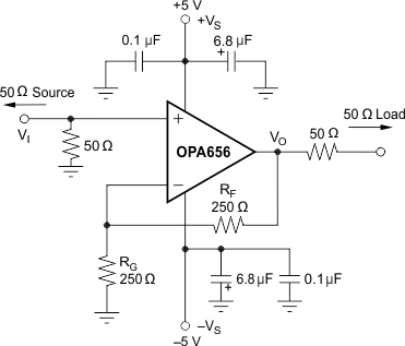
Figure 8-1 shows the noninverting gain of +2 V/V circuit used as the basis for most of the Typical Characteristics. Most of the curves were characterized using signal sources with 50‑Ω driving impedance, and with measurement equipment presenting a 50‑Ω load impedance. In Figure 8-1, the 50‑Ω shunt resistor at the VI terminal matches the source impedance of the test generator, while the 50‑Ω series resistor at the VO terminal provides a matching resistor for the measurement equipment load. Generally, data sheet voltage swing specifications are at the output pin (VO in Figure 8-1) while output power specifications are at the matched 50‑Ω load. The total 100-Ω load at the output combined with the 500‑Ω total feedback network load, presents the OPA656 with an effective output load of 83 Ω for the circuit of Figure 8-1.
 Figure 8-1 Noninverting G = +2 V/V Specifications and Test Circuit
Voltage-feedback operational amplifiers, unlike current feedback products, can use a wide range of resistor values to set the gain. To retain a controlled frequency response for the noninverting voltage amplifier of Figure 8-1, ensure that the parallel combination of RF || RG is always < 200 Ω. In the noninverting configuration, the parallel combination of RF || RG forms a pole with the parasitic input capacitance at the inverting node of the OPA656 (including layout parasitics). For best performance, ensure this pole is at a frequency greater than the closed-loop bandwidth for the OPA656. For this reason, TI recommends a direct short from the output to the inverting input for the unity-gain follower application.