ZHCSTX5B September 2000 – April 2024 OPA627 , OPA637
PRODMIX
- 1
- 1 特性
- 2 应用
- 3 说明
- 4 Pin Configuration and Functions
-
5 Specifications
- 5.1 Absolute Maximum Ratings
- 5.2 ESD Ratings
- 5.3 Recommended Operating Conditions
- 5.4 Thermal Information: OPA627
- 5.5 Thermal Information: OPA637
- 5.6 Electrical Characteristics: OPA627BU, OPA627AU
- 5.7 Electrical Characteristics: OPA627AM, OPA627BM, OPA627SM
- 5.8 Electrical Characteristics: OPA637
- 5.9 Typical Characteristics
- 6 Detailed Description
- 7 Application and Implementation
- 8 Device and Documentation Support
- 9 Revision History
- 10Mechanical, Packaging, and Orderable Information
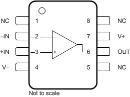
4 Pin Configuration and Functions
 Figure 4-1 D Package, 8-Pin SOIC (Top
View)
Figure 4-1 D Package, 8-Pin SOIC (Top
View)Table 4-1 Pin Functions: D (SOIC) Package
| PIN | TYPE | DESCRIPTION | |
|---|---|---|---|
| NO. | NAME | ||
| 1, 5, 8 | NC | — | No internal connection (can be left floating) |
| 2 | –IN | Input | Inverting input |
| 3 | +IN | Input | Noninverting input |
| 4 | V– | Power | Negative (lowest) power supply |
| 6 | OUT | Output | Output |
| 7 | V+ | Power | Positive (highest) power supply |
Figure 4-2 LMC Package, 8-Pin TO-99 (Top
View)
Table 4-2 Pin Functions: LMC (TO-99)
Package
| PIN | TYPE | DESCRIPTION | |
|---|---|---|---|
| NO. | NAME | ||
| 1, 5 | Offset Trim | — | Input offset voltage trim (float this pin if unused) |
| 2 | –IN | Input | Inverting input |
| 3 | +IN | Input | Noninverting input |
| 4 | V– | Power | Negative (lowest) power supply |
| 6 | OUT | Output | Output |
| 7 | V+ | Power | Positive (highest) power supply |
| 8 | NC | — | No internal connection (float this pin) |