ZHCSOR9A November   2021  – April 2022 OPA4H014-SEP

PRODUCTION DATA  

  1. 特性
  2. 应用
  3. 说明
  4. Revision History
  5. Pin Configuration and Functions
  6. Specifications
    1. 6.1 Absolute Maximum Ratings
    2. 6.2 ESD Ratings
    3. 6.3 Recommended Operating Conditions
    4. 6.4 Thermal Information
    5. 6.5 Electrical Characteristics
    6. 6.6 Typical Characteristics
  7. Detailed Description
    1. 7.1 Overview
    2. 7.2 Functional Block Diagram
    3. 7.3 Feature Description
      1. 7.3.1 Capacitive Load and Stability
      2. 7.3.2 Output Current Limit
      3. 7.3.3 Phase-Reversal Protection
      4. 7.3.4 Thermal Protection
    4. 7.4 Device Functional Modes
  8. Application and Implementation
    1. 8.1 Application Information
      1. 8.1.1 Noise Performance
        1. 8.1.1.1 Basic Noise Calculations
      2. 8.1.2 Electrical Overstress
      3. 8.1.3 EMI Rejection
      4. 8.1.4 EMIRR +IN Test Configuration
    2. 8.2 Typical Application
      1. 8.2.1 Design Requirements
      2. 8.2.2 Detailed Design Procedure
      3. 8.2.3 Application Curve
    3. 8.3 Power Supply Recommendations
    4. 8.4 Layout
      1. 8.4.1 Layout Guidelines
      2. 8.4.2 Layout Example
  9. Device and Documentation Support
    1. 9.1 Device Support
      1. 9.1.1 Development Support
        1. 9.1.1.1 PSpice® for TI
        2. 9.1.1.2 TINA-TI™ Simulation Software (Free Download)
        3. 9.1.1.3 Filter Design Tool
    2. 9.2 Documentation Support
      1. 9.2.1 Related Documentation
    3. 9.3 接收文档更新通知
    4. 9.4 支持资源
    5. 9.5 Trademarks
    6. 9.6 Electrostatic Discharge Caution
    7. 9.7 术语表
  10. 10Mechanical, Packaging, and Orderable Information

封装选项

机械数据 (封装 | 引脚)
散热焊盘机械数据 (封装 | 引脚)
订购信息

Typical Characteristics

at TA = 25°C, VS = ±9 V, RL = 2 kΩ connected to midsupply, and VCM = VOUT = midsupply (unless otherwise noted)

Table 6-1 Table of Graphs
DESCRIPTION FIGURE
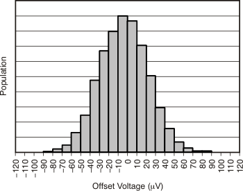
Offset Voltage Production Distribution Figure 6-1
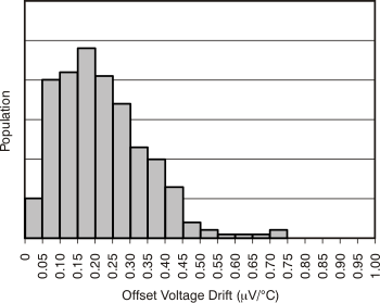
Offset Voltage Drift Distribution Figure 6-2
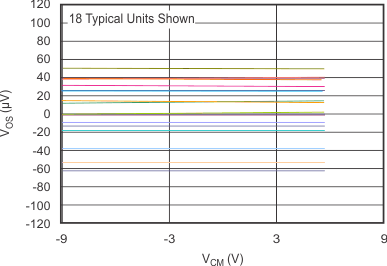
Offset Voltage vs Common-Mode Voltage (Maximum Supply) Figure 6-3
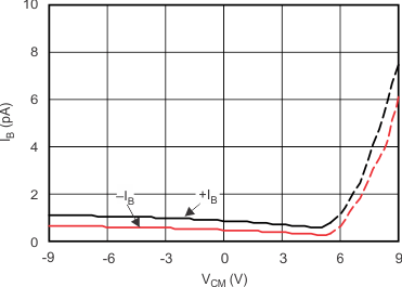
IB vs Common-Mode Voltage Figure 6-4
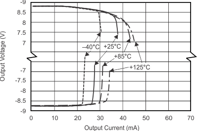
Output Voltage Swing vs Output Current Figure 6-5
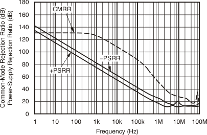
CMRR and PSRR vs Frequency (RTI) Figure 6-6
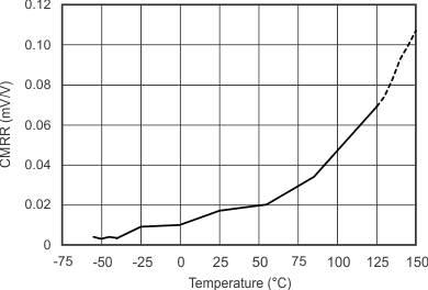
Common-Mode Rejection Ratio vs Temperature Figure 6-7
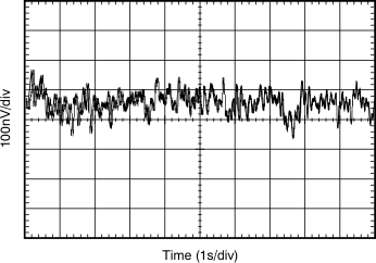
0.1-Hz to 10-Hz Noise Figure 6-8
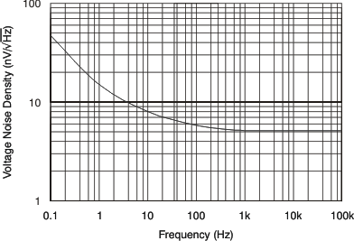
Input Voltage Noise Density vs Frequency Figure 6-9
THD+N Ratio vs Frequency (80-kHz AP Bandwidth) Figure 6-10
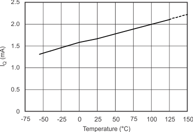
Quiescent Current vs Temperature Figure 6-11
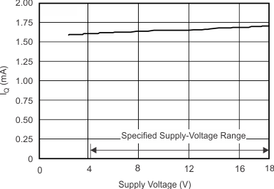
Quiescent Current vs Supply Voltage Figure 6-12
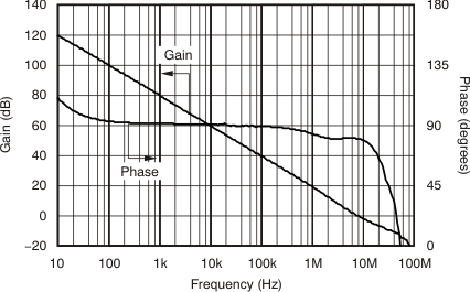
Gain and Phase vs Frequency Figure 6-13
Closed-Loop Gain vs Frequency Figure 6-14
Open-Loop Gain vs Temperature Figure 6-15
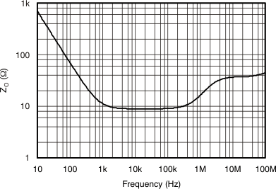
Open-Loop Output Impedance vs Frequency Figure 6-16
Small-Signal Overshoot vs Capacitive Load (G = 1) Figure 6-17
Small-Signal Overshoot vs Capacitive Load (G = –1) Figure 6-18
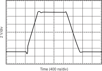
No Phase Reversal Figure 6-19
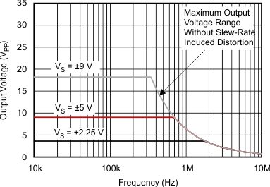
Maximum Output Voltage vs Frequency Figure 6-20
Positive Overload Recovery Figure 6-21
Negative Overload Recovery Figure 6-22
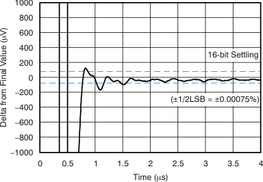
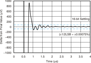
Large-Signal Positive and Negative Settling Time Figure 6-23, Figure 6-24
Small-Signal Step Response (G = 1) Figure 6-25
Small-Signal Step Response (G = –1) Figure 6-26
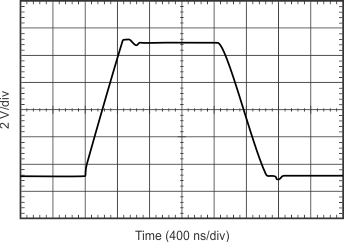
Large-Signal Step Response (G = 1) Figure 6-27
Large-Signal Step Response (G = –1) Figure 6-28
Short-Circuit Current vs Temperature Figure 6-29
Channel Separation vs Frequency Figure 6-30
GUID-9BCC19F2-4362-434D-8245-545697534B59-low.gif
 
Figure 6-1 Offset Voltage Production Distribution
GUID-1BE21F25-5E31-473F-8F83-FAA92679295E-low.gif
 
Figure 6-3 Offset Voltage vs Common-Mode Voltage
GUID-599A4BBF-9C21-4744-8665-1F2E74CF7E8C-low.gif
 
Figure 6-5 Output Voltage Swing vs Output Current
(Maximum Supply)
GUID-9110187F-4309-4A4C-B239-8928D13E6F50-low.gif
 
Figure 6-7 Common-Mode Rejection Ratio vs Temperature
GUID-50BAFA72-843F-4F3C-8969-FB4354B841C3-low.gif
 
Figure 6-9 Input Voltage Noise Density vs Frequency
GUID-2FB87FE0-3621-452B-B637-94D65EC24AAA-low.gif
 
Figure 6-11 Quiescent Current vs Temperature
GUID-B5F114BE-0E84-470E-AE08-2652D3094E75-low.gif
 
Figure 6-13 Gain and Phase vs Frequency
 
Figure 6-15 Open-Loop Gain vs Temperature
G = +1
Figure 6-17 Small-Signal Overshoot vs Capacitive Load
(100-mV Output Step)
 
 
Figure 6-19 No Phase Reversal
 G = –10
Figure 6-21 Positive Overload Recovery
GUID-F354357D-2B72-4819-AF60-C9CD4C66DB5C-low.gif
 
Figure 6-23 Large-Signal Positive Settling Time (10-V Step)
G = +1, CL = 100 pF
Figure 6-25 Small-Signal Step Response (100 mV)
GUID-FF4A68C0-88FF-4178-8D1E-5436365AA952-low.gif
 
Figure 6-27 Large-Signal Step Response
Short-circuiting may cause thermal shutdown;
see Application Information section
Figure 6-29 Short Circuit Current vs Temperature
GUID-8D25039F-B00D-4A7D-ABBD-EFEE50153E6C-low.gif
 
Figure 6-2 Offset Voltage Drift Distribution
GUID-CF982830-08BD-4E96-ACED-C8DDCDF018A7-low.gif
 
Figure 6-4 Bias Current vs Common-Mode Voltage
GUID-0D6EDBE7-4BA9-4A52-B3C0-76EC4D1E6529-low.gif
 
Figure 6-6 CMRR and PSRR vs Frequency (Referred to Input)
GUID-A9E2E08E-9364-4DEF-8F38-4C0714EDAA1F-low.gif
 
 
Figure 6-8 0.1-Hz to 10-Hz Noise
VOUT = 3 VRMS, BW = 80 kHz, RL = 2 kΩ
 
Figure 6-10 THD+N Ratio vs Frequency
GUID-F724214C-E259-4AAE-9A38-799B8ED57742-low.gif
 
Figure 6-12 Quiescent Current vs Supply Voltage
CL = 30 pF
Figure 6-14 Closed-Loop Gain vs Frequency
GUID-0F440C3F-16E9-4401-88BD-1B9D0B0C9DF0-low.gif
 
Figure 6-16 Open-Loop Output Impedance vs Frequency
G = –1
Figure 6-18 Small-Signal Overshoot vs Capacitive Load
(100-mV Output Step)
GUID-BED6234E-DCCD-4559-A826-3CE0C2F067BA-low.gif
 
Figure 6-20 Maximum Output Voltage vs Frequency
G = –10 
Figure 6-22 Negative Overload Recovery
GUID-23D98802-7B36-4A27-9A42-0552B7275DA4-low.gif
 
Figure 6-24 Large-Signal Negative Settling Time (10-V Step)
G = –1, CL = 100 pF
Figure 6-26 Small-Signal Step Response (100 mV)
GUID-AF1F2811-ED01-46A4-B43C-E718EE33F375-low.gif
 
Figure 6-28 Large-Signal Step Response
VOUT = 3 VRMS
G = +1
Figure 6-30 Channel Separation vs Frequency