ZHCSJ65A December 2018 – December 2019 OPA462
PRODUCTION DATA.
- 1 特性
- 2 应用
- 3 说明
- 4 修订历史记录
- 5 Pin Configuration and Functions
- 6 Specifications
- 7 Detailed Description
- 8 Application and Implementation
- 9 Power Supply Recommendations
- 10Layout
- 11器件和文档支持
- 12机械、封装和可订购信息
10.1.1 Thermally-Enhanced PowerPAD™ Package
The OPA462 comes in an 8-pin SO PowerPAD package that provides an extremely low thermal resistance, RθJC(bot), path between the die and the exterior of the package. This package features an exposed thermal pad that has direct thermal contact with the die. Thus, excellent thermal performance is achieved by providing a good thermal path away from the thermal pad.
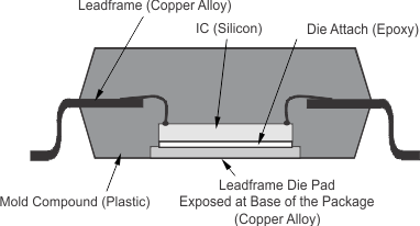
The OPA462 SO-8 PowerPAD is a standard-size SO-8 package constructed using a downset leadframe upon which the die is mounted, as Figure 67 shows. This arrangement results in the leadframe being exposed as a thermal pad on the underside of the package. The thermal pad on the bottom of the device can then be soldered directly to the PCB, using the PCB as a heat sink. In addition, plated-through holes (vias) provide a low thermal resistance heat flow path to the back side of the PCB. This architecture enhances the OPA462 power dissipation capability significantly, eliminates the use of bulky heat sinks and slugs traditionally used in thermal packages, and allows the OPA462 to be easily mounted using standard PCB assembly techniques.
NOTE
The SO-8 PowerPAD is pin-compatible with standard SO-8 packages, and as such, the OPA462 is a drop-in replacement for operational amplifiers in existing sockets. Always solder the PowerPAD to the PCB V– plane, even with applications that have low power dissipation. Solder the device to the PCB to provide the necessary thermal, mechanical, and electrical connections between the leadframe die pad and the PCB.
 Figure 67. Cross Section View of a PowerPAD™ Package