ZHCS509E November 2011 – June 2018 OPA180 , OPA2180 , OPA4180
PRODUCTION DATA.
- 1 特性
- 2 应用范围
- 3 说明
- 4 修订历史记录
- 5 Device Comparison Table
- 6 Pin Configuration and Functions
-
7 Specifications
- 7.1 Absolute Maximum Ratings
- 7.2 ESD Ratings
- 7.3 Recommended Operating Conditions
- 7.4 Thermal Information: OPA180
- 7.5 Thermal Information: OPA2180
- 7.6 Thermal Information: OPA4180
- 7.7 Electrical Characteristics: VS = ±2 V to ±18 V (VS = 4 V to 36 V)
- 7.8 Typical Characteristics: Table of Graphs
- 7.9 Typical Characteristics
- 8 Detailed Description
- 9 Application and Implementation
- 10Power Supply Recommendations
- 11Layout
- 12器件和文档支持
- 13机械、封装和可订购信息
6 Pin Configuration and Functions
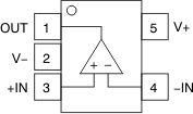
Pin Functions
| PIN | I/O | DESCRIPTION | |
|---|---|---|---|
| NAME | NO. | ||
| –IN | 4 | I | Inverting input |
| +IN | 3 | I | Noninverting input |
| OUT | 1 | O | Output |
| V– | 2 | — | Negative supply or ground (for single-supply operation) |
| V+ | 5 | — | Positive supply or ground (for single-supply operation) |
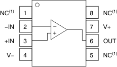
OPA180 D, DGK Packages
8-Pin SO,MSOP
Top View

1. NC- no internal connection
Pin Functions: OPA180
| PIN | DESCRIPTION | |
|---|---|---|
| NAME | NO. | |
| –IN | 2 | Inverting input |
| +IN | 3 | Noninverting input |
| NC | 1, 5, 8 | No connection |
| OUT | 6 | Output |
| V– | 4 | Negative power supply |
| V+ | 7 | Positive power supply |
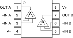
OPA2180 D, DGK Packages
8-Pin SOIC, VSSOP
Top View

Pin Functions: OPA2180
| PIN | DESCRIPTION | |
|---|---|---|
| NAME | NO. | |
| –IN A | 2 | Inverting input, channel A |
| +IN A | 3 | Noninverting input, channel A |
| –IN B | 6 | Inverting input, channel B |
| +IN B | 5 | Noninverting input, channel B |
| OUT A | 1 | Output, channel A |
| OUT B | 7 | Output, channel B |
| V– | 4 | Negative power supply |
| V+ | 8 | Positive power supply |
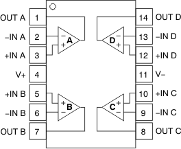
OPA4180 D, PW Packages
14-Pin SOIC, TSSOP
(Top View)

Pin Functions: OPA4180
| PIN | DESCRIPTION | |
|---|---|---|
| NAME | NO. | |
| –IN A | 2 | Inverting input, channel A |
| +IN A | 3 | Noninverting input, channel A |
| –IN B | 6 | Inverting input, channel B |
| +IN B | 5 | Noninverting input, channel B |
| –IN C | 9 | Inverting input, channel C |
| +IN C | 10 | Noninverting input, channel C |
| –IN D | 13 | Inverting input, channel D |
| +IN D | 12 | Noninverting input, channel D |
| OUT A | 1 | Output, channel A |
| OUT B | 7 | Output, channel B |
| OUT C | 8 | Output, channel C |
| OUT D | 14 | Output, channel D |
| V– | 11 | Negative supply or ground (for single-supply operation) |
| V+ | 4 | Positive supply or ground (for single-supply operation) |
