ZHCSLZ5D October   2020  – December 2023 OPA3S328

PRODUCTION DATA  

  1.   1
  2. 特性
  3. 应用
  4. 说明
  5. Pin Configuration and Functions
  6. Specifications
    1. 5.1 Absolute Maximum Ratings
    2. 5.2 ESD Ratings
    3. 5.3 Recommended Operating Conditions
    4. 5.4 Thermal Information
    5. 5.5 Electrical Characteristics
    6. 5.6 Timing Diagram
    7. 5.7 Typical Characteristics
  7. Parameter Measurement Information
    1. 6.1 Switch Characterization Configurations
  8. Detailed Description
    1. 7.1 Overview
    2. 7.2 Functional Block Diagram
    3. 7.3 Feature Description
      1. 7.3.1 Low Operating Voltage
      2. 7.3.2 Input and ESD Protection
      3. 7.3.3 Programmable Switches
      4. 7.3.4 Rail-to-Rail Input
      5. 7.3.5 Phase Reversal
    4. 7.4 Device Functional Modes
      1. 7.4.1 Power-Down Mode
  9. Application and Implementation
    1. 8.1 Application Information
      1. 8.1.1 Capacitive Load and Stability
      2. 8.1.2 EMI Susceptibility and Input Filtering
      3. 8.1.3 Transimpedance Amplifier
        1. 8.1.3.1 Optimizing the Transimpedance Circuit
    2. 8.2 Typical Application
      1. 8.2.1 Design Requirements
      2. 8.2.2 Detailed Design Procedure
      3. 8.2.3 Application Curve
    3. 8.3 Power Supply Recommendations
    4. 8.4 Layout
      1. 8.4.1 Layout Guidelines
      2. 8.4.2 Layout Example
  10. Device and Documentation Support
    1. 9.1 Device Support
      1. 9.1.1 Development Support
        1. 9.1.1.1 PSpice® for TI
        2. 9.1.1.2 TINA-TI™ 仿真软件(免费下载)
        3. 9.1.1.3 TI 参考设计
        4. 9.1.1.4 滤波器设计工具
    2. 9.2 Documentation Support
      1. 9.2.1 Related Documentation
    3. 9.3 接收文档更新通知
    4. 9.4 支持资源
    5. 9.5 Trademarks
    6. 9.6 静电放电警告
    7. 9.7 术语表
  11. 10Revision History
  12. 11Mechanical, Packaging, and Orderable Information

封装选项

机械数据 (封装 | 引脚)
散热焊盘机械数据 (封装 | 引脚)
订购信息

Input and ESD Protection

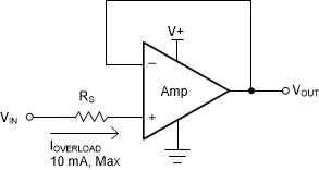
The OPA3S328 incorporates internal electrostatic discharge (ESD) protection circuits on all pins. In the case of input and output pins, this protection primarily consists of current-steering diodes connected between the input and power-supply pins. These ESD protection diodes also provide in-circuit input overdrive protection, provided that the current is limited to 10 mA. Many input signals are inherently current-limited to less than 10 mA; therefore, a limiting resistor is not required. Figure 7-1 shows how a series input resistor (RS) can be added to the driven input to limit the input current. The added resistor contributes thermal noise at the amplifier input; therefore, keep this value to a minimum in noise-sensitive applications.
GUID-20201001-CA0I-QSNK-BS2T-RCWRXPHBJ56C-low.gif Figure 7-1 Input Current Protection