ZHCSGW0E October   2017  – February 2020 OPA202 , OPA2202 , OPA4202

PRODUCTION DATA.  

  1. 特性
  2. 应用
  3. 说明
    1.     OPAx202 即使在直接驱动高容性负载时也表现优异
  4. 修订历史记录
  5. Pin Configuration and Functions
    1.     Pin Functions: OPA202
    2.     Pin Functions: OPA2202
    3.     Pin Functions: OPA4202
  6. Specifications
    1. 6.1 Absolute Maximum Ratings
    2. 6.2 ESD Ratings
    3. 6.3 Recommended Operating Conditions
    4. 6.4 Thermal Information: OPA202
    5. 6.5 Thermal Information: OPA2202
    6. 6.6 Thermal Information: OPA4202
    7. 6.7 Electrical Characteristics
    8. 6.8 Typical Characteristics
    9. 6.9 Typical Characteristics
  7. Detailed Description
    1. 7.1 Overview
    2. 7.2 Functional Block Diagram
    3. 7.3 Feature Description
      1. 7.3.1 Capacitive Load and Stability
      2. 7.3.2 Output Current Limit
      3. 7.3.3 Noise Performance
      4. 7.3.4 Phase-Reversal Protection
      5. 7.3.5 Thermal Protection
      6. 7.3.6 Electrical Overstress
      7. 7.3.7 EMI Rejection
      8. 7.3.8 EMIRR +IN Test Configuration
    4. 7.4 Device Functional Modes
  8. Application and Implementation
    1. 8.1 Application Information
      1. 8.1.1 Basic Noise Calculations
    2. 8.2 Typical Application
      1. 8.2.1 Design Requirements
      2. 8.2.2 Detailed Design Procedure
      3. 8.2.3 Application Curve
  9. Power Supply Recommendations
  10. 10Layout
    1. 10.1 Layout Guidelines
    2. 10.2 Layout Example
  11. 11器件和文档支持
    1. 11.1 器件支持
      1. 11.1.1 开发支持
        1. 11.1.1.1 TINA-TI(免费软件下载)
        2. 11.1.1.2 WEBENCH 滤波器设计器工具
        3. 11.1.1.3 TI 高精度设计
    2. 11.2 文档支持
      1. 11.2.1 相关文档
    3. 11.3 相关链接
    4. 11.4 接收文档更新通知
    5. 11.5 支持资源
    6. 11.6 商标
    7. 11.7 静电放电警告
    8. 11.8 Glossary
  12. 12机械、封装和可订购信息

封装选项

机械数据 (封装 | 引脚)
散热焊盘机械数据 (封装 | 引脚)
订购信息

Noise Performance

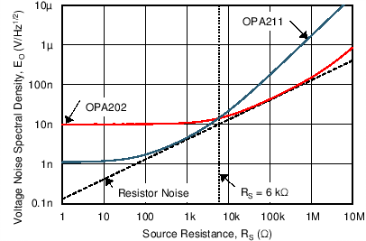
Figure 42 shows the total circuit noise for varying source impedances with the operational amplifier in a unity-gain configuration (with no feedback resistor network and therefore no additional noise contributions). The OPAx202 and OPA211 are shown with total circuit noise calculated. The op amp itself contributes a voltage noise component and a current noise component. The voltage noise is commonly modeled as a time-varying component of the offset voltage. The current noise is modeled as the time-varying component of the input bias current and reacts with the source resistance to create a voltage component of noise. Therefore, the lowest noise op amp for a given application depends on the source impedance. For low source impedance, current noise is negligible and voltage noise dominates. The OPAx202 have both low voltage noise and low current noise because of the super-beta bipolar junction transistor (super-β BJT) input of the op amp. As a result, the current noise contribution of the OPAx202 is negligible for most practical source impedances, which makes the series the better choice for applications with high source impedance.

The equation in Figure 42 shows the calculation of the total circuit noise with these parameters:

  • en = voltage noise
  • In = current noise
  • RS = source impedance
  • k = Boltzmann's constant = 1.38 × 10⁻²³ J/K
  • T = temperature in kelvins (K)

For more details on calculating noise, see Basic Noise Calculations.
OPA202 OPA2202 OPA4202 C302_SBOS812.png
NOTE: For source resistances (RS) greater than 6 kΩ, the OPAx202 is a lower-noise option compared to the OPA211, as shown in Figure 42.
Figure 42. Noise Performance of the OPAx202 vs the OPA211 in a Unity-Gain Buffer Configuration