ZHCSGW0E October 2017 – February 2020 OPA202 , OPA2202 , OPA4202
PRODUCTION DATA.
7.3.1 Capacitive Load and Stability
The dynamic characteristics of the OPAx202 are optimized for commonly encountered gains, loads, and operating conditions. The OPAx202 feature a patented output stage capable of driving large capacitive loads. In a unity-gain configuration, the series is capable of directly driving to 25 nF of pure capacitive load. Increase the gain to enhance the ability of the devices to drive greater capacitive loads. The particular op amp circuit configuration, layout, gain, and output loading are some of the factors to consider when establishing whether an amplifier is stable in operation.
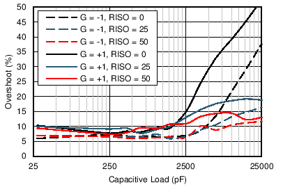
The combination of low closed-loop gain and high capacitive loads decreases the phase margin of the amplifier, and can lead to gain peaking or oscillations. As a result, heavier capacitive loads must be isolated from the output. Add a small resistor (ROUT equal to 50 Ω, for example) in series with the output to achieve isolation. Figure 40 shows the effects on small-signal overshoot for several capacitive loads and combinations of isolation resistance. See the Feedback Plots Define Op Amp AC Performance application bulletin for details of analysis techniques and application circuits, available for download from the www.TI.com. By using isolation resistors, driving capacitive loads of 100 nF and beyond is possible.
 Figure 40. Small-Signal Overshoot vs Capacitive Load (10-mV Output Step)
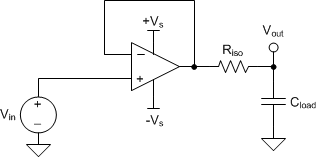
 For additional drive capability in unity-gain configurations, insert a small (10 Ω to 20 Ω) resistor (RISO) in series with the output to improve capacitive load drive, as shown in Figure 41. This resistor reduces ringing and maintains dc performance for purely capacitive loads. However, if a resistive load is in parallel with the capacitive load, then a voltage divider is created, which introduces a gain error at the output and reduces the output swing. The error is proportional to the ratio RISO / RL, and is generally negligible at low output levels. A high capacitive load drive makes the OPAx202 a great choice for applications such as reference buffers, MOSFET gate drives, and cable-shield drives. The circuit shown in Figure 41 uses an isolation resistor (RISO) to stabilize the output of an op amp. RISO modifies the open-loop gain of the system for increased phase margin. Table 2 lists the results using the OPAx202. For additional information on techniques to optimize and design using this circuit, TI Precision Design TIPD128 details complete design goals, simulation, and test results.
 Figure 41. Extending Capacitive Load Drive With the OPAx202
 Table 2. OPAx202 Capacitive Load Drive Solution Using Isolation Resistor Measured Results
| PARAMETER | MEASURED OVERSHOOT (%) | |||||
|---|---|---|---|---|---|---|
| INVERTING CONFIGURATION | NONINVERTING CONFIGURATION | |||||
| CLOAD (pF) | RISO = 0 Ω | RISO = 25 Ω | RISO = 50 Ω | RISO = 0 Ω | RISO = 25 Ω | RISO = 50 Ω |
| 31 | 8.6 | 6.6 | 6.6 | 9.3 | 9 | 9.4 |
| 251 | 6.7 | 6.4 | 6.7 | 8.9 | 8.9 | 8.9 |
| 421 | 6.4 | 6.3 | 6.6 | 8.8 | 8.8 | 8.7 |
| 641 | 6.7 | 6.3 | 6.5 | 8.1 | 8.8 | 8.5 |
| 1079 | 6.1 | 6.1 | 6.4 | 8.6 | 8.7 | 9.8 |
| 1539 | 6.4 | 6.3 | 6.1 | 8.9 | 10.3 | 10.1 |
| 2579 | 6.1 | 6.3 | 6.9 | 16 | 13.3 | 12 |
| 3949 | 8.1 | 7.9 | 8.3 | 25 | 16 | 14.1 |
| 6269 | 14.9 | 10.8 | 9.9 | 33.1 | 18.1 | 14.5 |
| 10139 | 21.8 | 13.5 | 10.8 | 40.2 | 19.1 | 15.4 |
| 15729 | 29.4 | 15.2 | 11.6 | 46.2 | 19.6 | 14.5 |
| 25069 | 37 | 16.5 | 12.3 | 52.6 | 19.2 | 13.9 |
| For step-by-step design procedure, circuit schematics, bill of materials, printed circuit board (PCB) files, simulation results, and test results, see TIPD128, Capacitive Load Drive Solution Using an Isolation Resistor verified reference design. |