ZHCSOD6E December 2003 – August 2023 OPA1632
PRODUCTION DATA
- 1
- 1 特性
- 2 应用
- 3 说明
- 4 Revision History
- 5 Pin Configuration and Functions
- 6 Specifications
- 7 Detailed Description
- 8 Application and Implementation
- 9 Device and Documentation Support
- 10Mechanical, Packaging, and Orderable Information
封装选项
机械数据 (封装 | 引脚)
散热焊盘机械数据 (封装 | 引脚)
- DGN|8
订购信息
8.4.1.2 Power Dissipation and Thermal Considerations
The OPA1632 does not have thermal shutdown protection. Make sure that the maximum junction temperature is not exceeded. Excessive junction temperature can degrade performance or cause permanent damage. For best performance and reliability, make sure that the junction temperature does not exceed the absolute maximum ratings for the junction temperature.
The thermal characteristics of the device are dictated by the package and the circuit board. Maximum power dissipation for a given package can be calculated using the following formula:
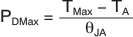
where:
- PDMax is the maximum power dissipation in the amplifier (W)
- TMax is the absolute maximum junction temperature (°C)
- TA is the ambient temperature (°C)
- θJA = θJC + θCA
- θJC is the thermal coefficient from the silicon junctions to the case (°C/W)
- θCA is the thermal coefficient from the case to ambient air (°C/W)
For systems where heat dissipation is more critical, the OPA1632 is offered in an HVSSOP-8 (DGN) PowerPAD integrated circuit package. The thermal coefficient for the PowerPAD integrated circuit package is substantially improved over the traditional SO package. Maximum power dissipation levels are depicted in Figure 8-6 for the two packages. The data for the DGN package assume a board layout that follows the layout guidelines listed in Section 8.4.1.1.
 Figure 8-6 Maximum
Power Dissipation vs Ambient Temperature
Figure 8-6 Maximum
Power Dissipation vs Ambient Temperature