ZHCSNP1A March 2021 – October 2021 MCT8316Z
PRODUCTION DATA
- 1 特性
- 2 应用
- 3 说明
- 4 Revision History
- 5 Device Comparison Table
- 6 Pin Configuration and Functions
- 7 Specifications
-
8 Detailed Description
- 8.1 Overview
- 8.2 Functional Block Diagram
- 8.3
Feature Description
- 8.3.1 Output Stage
- 8.3.2 PWM Control Mode (1x PWM Mode)
- 8.3.3 Device Interface Modes
- 8.3.4 Step-Down Mixed-Mode Buck Regulator
- 8.3.5 AVDD Linear Voltage Regulator
- 8.3.6 Charge Pump
- 8.3.7 Slew Rate Control
- 8.3.8 Cross Conduction (Dead Time)
- 8.3.9 Propagation Delay
- 8.3.10 Pin Diagrams
- 8.3.11 Active Demagnetization
- 8.3.12 Cycle-by-Cycle Current Limit
- 8.3.13 Hall Comparators (Analog Hall Inputs)
- 8.3.14 Advance Angle
- 8.3.15 FGOUT Signal
- 8.3.16
Protections
- 8.3.16.1 VM Supply Undervoltage Lockout (NPOR)
- 8.3.16.2 AVDD Undervoltage Lockout (AVDD_UV)
- 8.3.16.3 BUCK Undervoltage Lockout (BUCK_UV)
- 8.3.16.4 VCP Charge Pump Undervoltage Lockout (CPUV)
- 8.3.16.5 Overvoltage Protections (OV)
- 8.3.16.6 Overcurrent Protection (OCP)
- 8.3.16.7 Buck Overcurrent Protection
- 8.3.16.8 Motor Lock (MTR_LOCK)
- 8.3.16.9 Thermal Warning (OTW)
- 8.3.16.10 Thermal Shutdown (OTS)
- 8.4 Device Functional Modes
- 8.5 SPI Communication
- 8.6 Register Map
- 9 Application and Implementation
- 10Power Supply Recommendations
- 11Layout
- 12Device and Documentation Support
8.5.1.1 SPI Format
The SDI input data word is 16 bits long and consists of the following format:
- 1 read or write bit, W (bit B15)
- 6 address bits, A (bits B14 through B9)
- Parity bit, P (bit B8). Parity bit is set such that the SDI input data word has even number of 1s and 0s
- 8 data bits, D (bits B7 through B0)
The SDO output data word is 16 bits long and the first 8 bits are status bits. The data word is the content of the register being accessed.
For a write command (W0 = 0), the response word on the SDO pin is the data currently in the register being written to.
For a read command (W0 = 1), the response word is the data currently in the register being read.
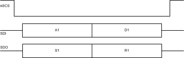 Figure 8-46
  Figure 8-47
 | R/W | ADDRESS | Parity | DATA | ||||||||||||
|---|---|---|---|---|---|---|---|---|---|---|---|---|---|---|---|
| B15 | B14 | B13 | B12 | B11 | B10 | B9 | B8 | B7 | B6 | B5 | B4 | B3 | B2 | B1 | B0 |
| W0 | A5 | A4 | A3 | A2 | A1 | A0 | P | D7 | D6 | D5 | D4 | D3 | D2 | D1 | D0 |
| STATUS | DATA | ||||||||||||||
|---|---|---|---|---|---|---|---|---|---|---|---|---|---|---|---|
| B15 | B14 | B13 | B12 | B11 | B10 | B9 | B8 | B7 | B6 | B5 | B4 | B3 | B2 | B1 | B0 |
| S7 | S6 | S5 | S4 | S3 | S2 | S1 | S0 | D7 | D6 | D5 | D4 | D3 | D2 | D1 | D0 |
 Figure 8-48 SPI Secondary Timing Diagram
SPI Error Handling
SPI Frame Error (SPI_SCLK_FLT: If the nSCS gets deasserted before the end of 16-bit frame, SPI frame error is detected and SPI_SCLK_FLT bit is set in STAT2. The SPI_SCLK_FLT status bit is latched and can be cleared when a clear faults command is issued either through the CLR_FLT bit or an nSLEEP reset pulse
SPI Address Error (SPI_ADDR_FLT): If an invalid address is provided in the ADDR field of the input SPI data on SDI, SPI address error is detected and SPI_ADDR_FLT bit in STAT2 is set. Invalid address is any address that is not defined in Section 8.6 i.e. address not falling in the range of address 0x0 to 0xC. The SPI_ADDR_FLT status bit is latched and can be cleared when a clear faults command is issued either through the CLR_FLT bit or an nSLEEP reset pulse