ZHCSNP1A March   2021  – October 2021 MCT8316Z

PRODUCTION DATA  

  1. 特性
  2. 应用
  3. 说明
  4. Revision History
  5. Device Comparison Table
  6. Pin Configuration and Functions
    1.     Pin Functions
  7. Specifications
    1. 7.1 Absolute Maximum Ratings
    2. 7.2 ESD Ratings
    3. 7.3 Recommended Operating Conditions
    4. 7.4 Thermal Information
    5. 7.5 Electrical Characteristics
    6. 7.6 SPI Timing Requirements
    7. 7.7 SPI Secondary Mode Timings
    8. 7.8 Typical Characteristics
  8. Detailed Description
    1. 8.1 Overview
    2. 8.2 Functional Block Diagram
    3. 8.3 Feature Description
      1. 8.3.1  Output Stage
      2. 8.3.2  PWM Control Mode (1x PWM Mode)
        1. 8.3.2.1 Analog Hall Input Configuration
        2. 8.3.2.2 Digital Hall Input Configuration
        3. 8.3.2.3 Asynchronous Modulation
        4. 8.3.2.4 Synchronous Modulation
        5. 8.3.2.5 Motor Operation
      3. 8.3.3  Device Interface Modes
        1. 8.3.3.1 Serial Peripheral Interface (SPI)
        2. 8.3.3.2 Hardware Interface
      4. 8.3.4  Step-Down Mixed-Mode Buck Regulator
        1. 8.3.4.1 Buck in Inductor Mode
        2. 8.3.4.2 Buck in Resistor mode
        3. 8.3.4.3 Buck Regulator with External LDO
        4. 8.3.4.4 AVDD Power Sequencing on Buck Regulator
        5. 8.3.4.5 Mixed mode Buck Operation and Control
      5. 8.3.5  AVDD Linear Voltage Regulator
      6. 8.3.6  Charge Pump
      7. 8.3.7  Slew Rate Control
      8. 8.3.8  Cross Conduction (Dead Time)
      9. 8.3.9  Propagation Delay
        1. 8.3.9.1 Driver Delay Compensation
      10. 8.3.10 Pin Diagrams
        1. 8.3.10.1 Logic Level Input Pin (Internal Pulldown)
        2. 8.3.10.2 Logic Level Input Pin (Internal Pullup)
        3. 8.3.10.3 Open Drain Pin
        4. 8.3.10.4 Push Pull Pin
        5. 8.3.10.5 Four Level Input Pin
        6. 8.3.10.6 Seven Level Input Pin
      11. 8.3.11 Active Demagnetization
        1. 8.3.11.1 Automatic Synchronous Rectification Mode (ASR Mode)
          1. 8.3.11.1.1 Automatic Synchronous Rectification in Commutation
          2. 8.3.11.1.2 Automatic Synchronous Rectification in PWM Mode
        2. 8.3.11.2 Automatic Asynchronous Rectification Mode (AAR Mode)
      12. 8.3.12 Cycle-by-Cycle Current Limit
        1. 8.3.12.1 Cycle by Cycle Current Limit with 100% Duty Cycle Input
      13. 8.3.13 Hall Comparators (Analog Hall Inputs)
      14. 8.3.14 Advance Angle
      15. 8.3.15 FGOUT Signal
      16. 8.3.16 Protections
        1. 8.3.16.1  VM Supply Undervoltage Lockout (NPOR)
        2. 8.3.16.2  AVDD Undervoltage Lockout (AVDD_UV)
        3. 8.3.16.3  BUCK Undervoltage Lockout (BUCK_UV)
        4. 8.3.16.4  VCP Charge Pump Undervoltage Lockout (CPUV)
        5. 8.3.16.5  Overvoltage Protections (OV)
        6. 8.3.16.6  Overcurrent Protection (OCP)
          1. 8.3.16.6.1 OCP Latched Shutdown (OCP_MODE = 00b)
          2. 8.3.16.6.2 OCP Automatic Retry (OCP_MODE = 01b)
          3. 8.3.16.6.3 OCP Report Only (OCP_MODE = 10b)
          4. 8.3.16.6.4 OCP Disabled (OCP_MODE = 11b)
        7. 8.3.16.7  Buck Overcurrent Protection
        8. 8.3.16.8  Motor Lock (MTR_LOCK)
          1. 8.3.16.8.1 MTR_LOCK Latched Shutdown (MTR_LOCK_MODE = 00b)
          2. 8.3.16.8.2 MTR_LOCK Automatic Retry (MTR_LOCK_MODE = 01b)
          3. 8.3.16.8.3 MTR_LOCK Report Only (MTR_LOCK_MODE= 10b)
          4. 8.3.16.8.4 MTR_LOCK Disabled (MTR_LOCK_MODE = 11b)
          5. 8.3.16.8.5 77
        9. 8.3.16.9  Thermal Warning (OTW)
        10. 8.3.16.10 Thermal Shutdown (OTS)
    4. 8.4 Device Functional Modes
      1. 8.4.1 Functional Modes
        1. 8.4.1.1 Sleep Mode
        2. 8.4.1.2 Operating Mode
        3. 8.4.1.3 Fault Reset (CLR_FLT or nSLEEP Reset Pulse)
      2. 8.4.2 DRVOFF functionality
    5. 8.5 SPI Communication
      1. 8.5.1 Programming
        1. 8.5.1.1 SPI Format
    6. 8.6 Register Map
      1. 8.6.1 STATUS Registers
      2. 8.6.2 CONTROL Registers
  9. Application and Implementation
    1. 9.1 Application Information
    2. 9.2 Hall Sensor Configuration and Connection
      1. 9.2.1 Typical Configuration
      2. 9.2.2 Open Drain Configuration
      3. 9.2.3 Series Configuration
      4. 9.2.4 Parallel Configuration
    3. 9.3 Typical Applications
      1. 9.3.1 Three-Phase Brushless-DC Motor Control With Current Limit
        1. 9.3.1.1 Detailed Design Procedure
          1. 9.3.1.1.1 Motor Voltage
          2. 9.3.1.1.2 Using Active Demagnetization
          3. 9.3.1.1.3 Using Delay Compensation
          4. 9.3.1.1.4 Using the Buck Regulator
          5. 9.3.1.1.5 Power Dissipation and Junction Temperature Losses
        2. 9.3.1.2 Application Curves
  10. 10Power Supply Recommendations
    1. 10.1 Bulk Capacitance
  11. 11Layout
    1. 11.1 Layout Guidelines
    2. 11.2 Layout Example
    3. 11.3 Thermal Considerations
      1. 11.3.1 Power Dissipation
  12. 12Device and Documentation Support
    1. 12.1 支持资源
    2. 12.2 Trademarks
    3. 12.3 Electrostatic Discharge Caution
    4. 12.4 术语表

封装选项

机械数据 (封装 | 引脚)
散热焊盘机械数据 (封装 | 引脚)
订购信息
Using Active Demagnetization

Active demagnetization reduces power losses in the device by turning on the MOSFETs automatically when the body diode starts conducting to reduce diode conduction losses. It is used in trapezoidal commutation when switching commutation states (turning a high-side MOSFET off and another high-side MOSFET on while keeping a low-side MOSFET on). Active demagnetization is enabled when EN_ASR and EN_AAR bits are set in the SPI variant or MODE pin is set to Mode 5, Mode 6, or Mode 7 in the H/W variant.

When switching commutation states with active demagnetization disabled, dead time is inserted and the low-side MOSFET’s body diode conducts while turning another high-side MOSFET on to continue sourcing current through the motor. This conduction period causes higher power losses due to the forward-bias voltage of the diode and slower dissipation of current. Figure 9-7 shows the body diode conducting when switching commutation states.
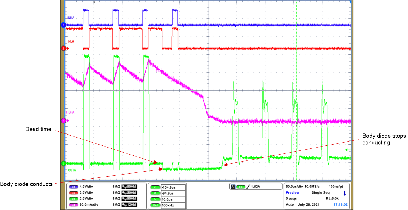
GUID-20210901-SS0I-MJCQ-XK8S-29RQK1DPQD6F-low.pngFigure 9-7 Active demagnetization disabled in MCT8316Z

When active demagnetization is enabled, the AD_HS and AD_LS comparators detect when the sense FET voltage is higher or lower than the programmed threshold. After the dead time period, if the threshold is exceeded for a fixed amount of time, the body diode is conducting and the logic core turns the low-side FET on to provide a conduction path with smaller power losses. Once the VDS voltage is below the comparator threshold, the MOSFET turns off and current briefly conducts through the body diode until the current completely decays to zero. This is shown in Figure 9-8.
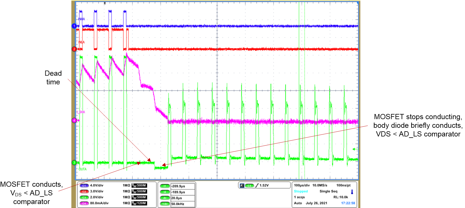
GUID-20210820-SS0I-X7G8-NH52-10DFBR8BZDV4-low.pngFigure 9-8 Active demagnetization enabled in MCT8316Z