ZHCSDH0C December 2014 – January 2018 LP3907-Q1
PRODUCTION DATA.
- 1 特性
- 2 应用
- 3 说明
- 4 修订历史记录
- 5 器件比较 台式机
- 6 Pin Configuration and Functions
-
7 Specifications
- 7.1 Absolute Maximum Ratings
- 7.2 ESD Ratings
- 7.3 Recommended Operating Conditions (Bucks)
- 7.4 Thermal Information
- 7.5 General Electrical Characteristics
- 7.6 Low Dropout Regulators, LDO1 And LDO2
- 7.7 Buck Converters SW1, SW2
- 7.8 I/O Electrical Characteristics
- 7.9 Power-On Reset (POR) Threshold/Function
- 7.10 I2C Interface Timing Requirements
- 7.11 Typical Characteristics — LDO
- 7.12 Typical Characteristics — Bucks
- 7.13 Typical Characteristics — Buck1
- 7.14 Typical Characteristics — Buck2
- 7.15 Typical Characteristics — Bucks
-
8 Detailed Description
- 8.1 Overview
- 8.2 Functional Block Diagram
- 8.3
Feature Description
- 8.3.1 DC-DC Converters
- 8.3.2
SW1, SW2: Synchronous Step-Down Magnetic DC-DC Converters
- 8.3.2.1 Functional Description
- 8.3.2.2 Circuit Operation Description
- 8.3.2.3 PWM Operation
- 8.3.2.4 Internal Synchronous Rectification
- 8.3.2.5 Current Limiting
- 8.3.2.6 PFM Operation
- 8.3.2.7 SW1, SW2 Operation
- 8.3.2.8 SW1, SW2 Control Registers
- 8.3.2.9 Soft Start
- 8.3.2.10 Low Dropout Operation
- 8.3.2.11 Flexible Power Sequencing of Multiple Power Supplies
- 8.3.2.12 Power-Up Sequencing Using the EN_T Function
- 8.3.3 Flexible Power-On Reset (Power Good with Delay)
- 8.3.4 Undervoltage Lockout
- 8.4 Device Functional Modes
- 8.5 Programming
- 8.6
Register Maps
- 8.6.1
LP3907-Q1 Control Registers
- 8.6.1.1 Interrupt Status Register (ISRA) 0x02
- 8.6.1.2 Control 1 Register (SCR1) 0x07
- 8.6.1.3 EN_DLY Preset Delay Sequence After EN_T Assertion
- 8.6.1.4 Buck and LDO Output Voltage Enable Register (BKLDOEN) – 0x10
- 8.6.1.5 Buck and LDO Status Register (BKLDOSR) – 0x11
- 8.6.1.6 Buck Voltage Change Control Register 1 (VCCR) – 0x20
- 8.6.1.7 Buck1 Target Voltage 1 Register (B1TV1) – 0x23
- 8.6.1.8 Buck1 Target Voltage 2 Register (B1TV2) – 0x24
- 8.6.1.9 Buck1 Ramp Control Register (B1RC) - 0x25
- 8.6.1.10 Buck2 Target Voltage 1 Register (B2TV1) – 0x29
- 8.6.1.11 Buck2 Target Voltage 2 Register (B2TV2) – 0x2A
- 8.6.1.12 Buck2 Ramp Control Register (B2RC) - 0x2B
- 8.6.1.13 Buck Function Register (BFCR) – 0x38
- 8.6.1.14 LDO1 Control Register (LDO1VCR) – 0x39
- 8.6.1.15 LDO2 Control Register (LDO2VCR) – 0x3A
- 8.6.1
LP3907-Q1 Control Registers
- 9 Application and Implementation
- 10Power Supply Recommendations
- 11Layout
- 12器件和文档支持
- 13机械、封装和可订购信息
封装选项
机械数据 (封装 | 引脚)
散热焊盘机械数据 (封装 | 引脚)
- RTW|24
订购信息
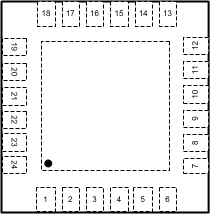
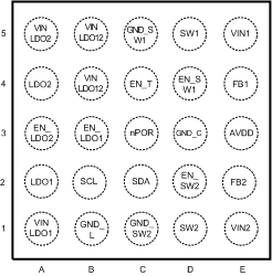
6 Pin Configuration and Functions
WQFN (RTW)
24 Leads
Top View

DSBGA (YZR)
25 Pins
Top View

Pin Functions
| PIN | I/O | TYPE(1) | DESCRIPTION | ||
|---|---|---|---|---|---|
| WQFN NUMBER | DSBGA NUMBER | NAME | |||
| 1 | B4, B5 | VINLDO12 | I | PWR | Analog Power for Internal Functions (VREF, BIAS, I2C, Logic) |
| 2 | C4 | EN_T | I | D | Enable for preset power on sequence. (See .) |
| 3 | C3 | nPOR | O | D | nPOR Power on reset pin for both Buck1 and Buck 2. Open drain logic output 100-kΩ pullup resistor. nPOR is pulled to ground when the voltages on these supplies are not good. See Flexible Power-On Reset (Power Good with Delay) section for more info. |
| 4 | C5 | GND_SW1 | G | G | Buck1 NMOS Power Ground |
| 5 | D5 | SW1 | O | PWR | Buck1 switcher output pin |
| 6 | E5 | VIN1 | I | PWR | Power in from either DC source or Battery to Buck1 |
| 7 | D4 | ENSW1 | I | D | Enable Pin for Buck1 switcher, a logic HIGH enables Buck1 |
| 8 | E4 | FB1 | I | A | Buck1 input feedback terminal |
| 9 | D3 | GND_C | G | G | Non switching core ground pin |
| 10 | E3 | AVDD | I | PWR | Analog Power for Buck converters |
| 11 | E2 | FB2 | I | A | Buck2 input feedback terminal |
| 12 | D2 | ENSW2 | I | D | Enable Pin for Buck2 switcher, a logic HIGH enables Buck2 |
| 13 | E1 | VIN2 | I | PWR | Power in from either DC source or Battery to Buck2 |
| 14 | D1 | SW2 | O | PWR | Buck2 switcher output pin |
| 15 | C1 | GND_SW2 | G | G | Buck2 NMOS Power ground |
| 16 | C2 | SDA | I/O | D | I2C Data (bidirectional) |
| 17 | B2 | SCL | I | D | I2C Clock |
| 18 | B1 | GND_L | G | G | LDO ground |
| 19 | A1 | VINLDO1 | I | PWR | Power in from either DC source or battery to input terminal to LDO1 |
| 20 | A2 | LDO1 | O | PWR | LDO1 Output |
| 21 | B3 | ENLDO1 | I | D | LDO1 enable pin, a logic HIGH enables the LDO1 |
| 22 | A3 | ENLDO2 | I | D | LDO2 enable pin, a logic HIGH enables the LDO2 |
| 23 | A4 | LDO2 | O | PWR | LDO2 Output |
| 24 | A5 | VINLDO2 | I | PWR | Power in from either DC source or battery to input terminal to LDO2. |
| DAP | DAP | GND | GND | Connection isn't necessary for electrical performance, but it is recommended for better thermal dissipation. | |
(1) A: Analog Pin D: Digital Pin G: Ground Pin PWR: Power Pin I: Input Pin I/O: Input/Output Pin O: Output Pin.