ZHCSHO0C February 2018 – March 2023 LMZM23600
PRODUCTION DATA
- 1 特性
- 2 应用
- 3 说明
- 4 Revision History
- 5 Device Comparison
- 6 Pin Configuration and Functions
- 7 Specifications
- 8 Detailed Description
- 9 Application and Implementation
- 10Device and Documentation Support
- 11Mechanical, Packaging, and Orderable Information
9.2.2.6 VIN Divider and Enable
If the application requires custom input UVLO level higher than the internal UVLO, a voltage divider can be connected from VIN to the EN terminal to set the turnon threshold.
 Figure 9-5 Enable Divider to Set External UVLO Threshold
Choose the top resistor RENB between 10 kΩ and 50 kΩ and calculate the RENT according to Equation 3.
Equation 3. 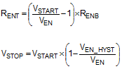
where
- VSTART is the rising input voltage level at which switching starts. Choose this value based on the application requirements.
- VSTOP is the input voltage at which switching stops
- VEN is the rising threshold on EN; see Electrical Characteristics
- VEN_HYST is the hysteresis on the EN threshold; see Electrical Characteristics