ZHCSD60D June 2012 – August 2018 LMZ20502
PRODUCTION DATA.
- 1 特性
- 2 应用
- 3 说明
- 4 修订历史记录
- 5 Pin Configuration and Functions
- 6 Specifications
- 7 Detailed Description
- 8 Application and Implementation
- 9 Power Supply Recommendations
- 10Layout
- 11器件和文档支持
- 12机械、封装和可订购信息
8.2.1.5 Maximum Ambient Temperature
As with any power conversion device, the LMZ20502 will dissipate internal power while operating. The effect of this power dissipation is to raise the internal temperature of the converter, above ambient. The internal die temperature is a function of the ambient temperature, the power loss and the effective thermal resistance RθJA of the device and PCB combination. The maximum internal die temperature for the LMZ20502 is 125°C, thus establishing a limit on the maximum device power dissipation and therefore load current at high ambient temperatures. Equation 3 shows the relationships between the important parameters.

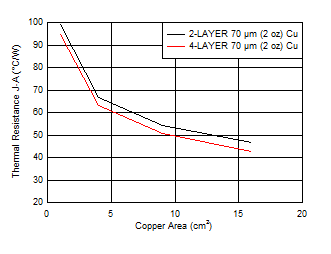
It is easy to see that larger ambient temperatures and larger values of RθJA will reduce the maximum available output current. As stated in SPRA953, the values given in the Thermal Information table are not valid for design purposes and must not be used to estimate the thermal performance of the application. The values reported in that table were measured under a specific set of conditions that never obtain in an actual application. The effective RθJA is a critical parameter and depends on many factors such as power dissipation, air temperature, PCB area, copper heatsink area, air flow, and adjacent component placement. The resources found in Table 3 can be used as a guide to estimate the RθJA for a given application environment. A typical example of RθJA versus copper board area is shown in Figure 18 . The copper area in this graph is that for each layer; the inner layers are 1 oz. (35µm). An RθJA of 44°C/W is the approximate value for the LMZ20502 evaluation board. The efficiency found in the equation, η, should be taken at the elevated ambient temperature. For the LMZ20502 the efficiency is about two to three percent lower at high temperatures. Therefore, a slightly lower value than the typical efficiency can be used in the calculation. In this way Equation 3 can be used to estimate the maximum output current for a given ambient, or to estimate the maximum ambient for a given load current.
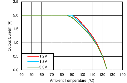
A typical curve of maximum load current vs. ambient temperature is shown in Figure 19. This graph assumes a RθJA of 44°C/W and an input voltage of 5 V.
 Figure 18. RθJA versus Copper Board Area
  Figure 19. Maximum Output Current Vs. Ambient Temperature, RθJA = 44°C/W, VIN = 5 V