ZHCSD60D June 2012 – August 2018 LMZ20502
PRODUCTION DATA.
- 1 特性
- 2 应用
- 3 说明
- 4 修订历史记录
- 5 Pin Configuration and Functions
- 6 Specifications
- 7 Detailed Description
- 8 Application and Implementation
- 9 Power Supply Recommendations
- 10Layout
- 11器件和文档支持
- 12机械、封装和可订购信息
7.4.2 PFM Operation
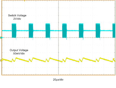
When in AUTO mode, and at light loads, the device enters PFM. The regulator estimates the load current by measuring both the high side and low side switch currents. This estimate is only approximate, and the exact load current threshold, to trigger PFM, can vary greatly with input and output voltage. The Application Curves show mode change thresholds for several typical operating points. When the regulator detects this threshold, the reference voltage is increased by approximately 10 mV. This causes the output voltage to rise to meet the new regulation point. When this point is reached, the converter stops switching and much of the internal circuitry is shut off, while the reference is returned to the PWM value. This saves supply current while the output voltage naturally starts to fall under the influence of the load current. When the output voltage reaches the PWM regulation point, switching is again started and the reference voltage is again increased by about 10 mV; thus starting the next cycle. Typical waveforms are shown in Figure 14:
 Figure 14. Typical PFM Mode Waveforms: VIN = 3.6 V,
VOUT = 1.8 V, IOUT = 10 mA
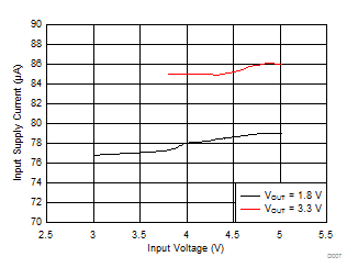
 Figure 15. Typical No Load Input Supply Current
 The actual output voltage ripple will depend on the feedback divider ratio and on the delay in the PFM comparator. The frequency of the PFM "bursts" will depend on the input voltage, output voltage, load and output capacitor. Within each "burst" the device switches at 3 MHz (typ.). If the load current increases above the threshold, normal PWM operation is resumed. This mode provides high light load efficiency by reducing the amount of supply current required to regulate the output at small load currents. This mode trades off very good light load efficiency for larger output voltage ripple and variable switching frequency. An example of the typical input supply current, while regulating with no load, is shown in Figure 15.
Because of normal part-to-part variation, the LMZ20502 may not switch into PFM mode at high input voltages. This may be seen with output voltages of about 1.2 V and below, at input voltages of about 4.2 V and above.