ZHCSGT2C November   2016  – August 2021 LMS3635-Q1 , LMS3655-Q1

PRODUCTION DATA  

  1. 特性
  2. 应用
  3. 说明
  4. Revision History
  5. Device Comparison Tables
  6. Pin Configuration and Functions
  7. Specifications
    1. 7.1 Absolute Maximum Ratings
    2. 7.2 ESD Ratings
    3. 7.3 Recommended Operating Conditions
    4. 7.4 Thermal Information
    5. 7.5 Thermal Information (for Device Mounted on PCB)
    6. 7.6 Electrical Characteristics
    7. 7.7 System Characteristics
    8. 7.8 Timing Requirements
    9. 7.9 Typical Characteristics
  8. Detailed Description
    1. 8.1 Overview
    2. 8.2 Functional Block Diagram
      1. 8.2.1 Control Scheme
    3. 8.3 Feature Description
      1. 8.3.1 RESET Flag Output
      2. 8.3.2 Enable and Start-Up
      3. 8.3.3 Soft-Start Function
      4. 8.3.4 Current Limit
      5. 8.3.5 Hiccup Mode
      6. 8.3.6 Synchronizing Input
      7. 8.3.7 Undervoltage Lockout (UVLO) and Thermal Shutdown (TSD)
      8. 8.3.8 Input Supply Current
    4. 8.4 Device Functional Modes
      1. 8.4.1 AUTO Mode
      2. 8.4.2 FPWM Mode
      3. 8.4.3 Dropout
      4. 8.4.4 Spread-Spectrum Operation
  9. Application and Implementation
    1. 9.1 Application Information
    2. 9.2 Typical Applications
      1. 9.2.1 General Application
        1. 9.2.1.1 Design Requirements
        2. 9.2.1.2 Detailed Design Procedure
          1. 9.2.1.2.1 Custom Design With WEBENCH® Tools
          2. 9.2.1.2.2 External Components Selection
            1. 9.2.1.2.2.1 Input Capacitors
            2. 9.2.1.2.2.2 Output Inductors and Capacitors
              1. 9.2.1.2.2.2.1 Inductor Selection
              2. 9.2.1.2.2.2.2 Output Capacitor Selection
          3. 9.2.1.2.3 Setting the Output Voltage
          4. 9.2.1.2.4 FB for Adjustable Output
          5. 9.2.1.2.5 VCC
          6. 9.2.1.2.6 BIAS
          7. 9.2.1.2.7 CBOOT
          8. 9.2.1.2.8 Maximum Ambient Temperature
        3. 9.2.1.3 Application Curves
      2. 9.2.2 Fixed 5-V Output for USB-Type Applications
        1. 9.2.2.1 Design Requirements
        2. 9.2.2.2 Detailed Design Procedure
        3. 9.2.2.3 Application Curves
      3. 9.2.3 Fixed 3.3-V Output
        1. 9.2.3.1 Design Requirements
        2. 9.2.3.2 Detailed Design Procedure
        3. 9.2.3.3 Application Curves
      4. 9.2.4 6-V Adjustable Output
        1. 9.2.4.1 Design Requirements
        2. 9.2.4.2 Detailed Design Procedure
        3. 9.2.4.3 Application Curves
    3. 9.3 Do's and Don't's
  10. 10Power Supply Recommendations
  11. 11Layout
    1. 11.1 Layout Guidelines
    2. 11.2 Layout Example
  12. 12Device and Documentation Support
    1. 12.1 Device Support
      1. 12.1.1 第三方产品免责声明
      2. 12.1.2 Development Support
        1. 12.1.2.1 Custom Design With WEBENCH® Tools
    2. 12.2 Documentation Support
      1. 12.2.1 Related Documentation
    3. 12.3 接收文档更新通知
    4. 12.4 支持资源
    5. 12.5 Trademarks
    6. 12.6 Electrostatic Discharge Caution
    7. 12.7 术语表
  13. 13Mechanical, Packaging, and Orderable Information

封装选项

机械数据 (封装 | 引脚)
散热焊盘机械数据 (封装 | 引脚)
订购信息

Dropout

The minimum off time influences the dropout performance of the buck regulator. As the input voltage is reduced, to near the output voltage, the off time of the high-side switch starts to approach the minimum value (see Section 7.6). Beyond this point the switching may become erratic or the output voltage falls out of regulation. To avoid this problem, the LMS36x5-Q1 automatically reduces the switching frequency to increase the effective duty cycle. This results in two specifications regarding dropout voltage, as shown in Section 7.7. One specification indicates when the switching frequency drops to 330 kHz. The other specification indicates when the output voltage has fallen to 3% of nominal. See the Section 9.2.2.3 for typical dropout values. Figure 8-10 and Figure 8-11 show the overall dropout characteristic for the 5-V option. Additional dropout information is discussed in Section 9.2.2.3 for 5-V output and in Section 9.2.3.3 for 3.3-V output.
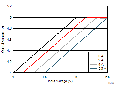
GUID-D37DA0B3-7FA4-4C33-8611-4DBB6C03D02B-low.gifFigure 8-10 Overall Dropout Characteristics (VOUT = 5 V)
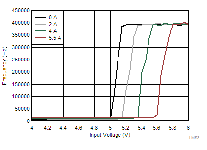
GUID-8DE09D2B-3662-4D55-AB51-DED578436460-low.gifFigure 8-11 Frequency Dropout Characteristics (VOUT = 5 V)