ZHCSMJ6B November 2020 – March 2021 LMK5C33216
PRODUCTION DATA
- 1 特性
- 2 应用
- 3 说明
- 4 Revision History
- 5 Device Comparison
- 6 Pin Configuration and Functions
- 7 Specifications
- 8 Parameter Measurement Information
-
9 Detailed Description
- 9.1 Overview
- 9.2 Functional Block Diagram
- 9.3
Feature Description
- 9.3.1 Oscillator Input (XO)
- 9.3.2 Reference Inputs
- 9.3.3 Clock Input Interfacing and Termination
- 9.3.4 Reference Input Mux Selection
- 9.3.5 Hitless Switching
- 9.3.6 Gapped Clock Support on Reference Inputs
- 9.3.7 Input Clock and PLL Monitoring, Status, and Interrupts
- 9.3.8
PLL Relationships
- 9.3.8.1 PLL Frequency Relationships
- 9.3.8.2 Analog PLLs (APLL1, APLL2, APLL3)
- 9.3.8.3 APLL Reference Paths
- 9.3.8.4 APLL Phase Frequency Detector (PFD) and Charge Pump
- 9.3.8.5 APLL Feedback Divider Paths
- 9.3.8.6 APLL Loop Filters (LF1, LF2, LF3)
- 9.3.8.7 APLL Voltage Controlled Oscillators (VCO1, VCO2, VCO3)
- 9.3.8.8 APLL VCO Clock Distribution Paths
- 9.3.8.9 DPLL Reference (R) Divider Paths
- 9.3.8.10 DPLL Time-to-Digital Converter (TDC)
- 9.3.8.11 DPLL Loop Filter (DLF)
- 9.3.8.12 DPLL Feedback (FB) Divider Path
- 9.3.9 Output Clock Distribution
- 9.3.10 Output Channel Muxes
- 9.3.11 Output Dividers (OD)
- 9.3.12 SYSREF
- 9.3.13 Output Delay
- 9.3.14 Clock Outputs (OUTx_P/N)
- 9.3.15 Glitchless Output Clock Start-Up
- 9.3.16 Clock Output Interfacing and Termination
- 9.3.17 Output Synchronization (SYNC)
- 9.3.18 Zero-Delay Mode (ZDM) Synchronization
- 9.3.19 Time of Day (ToD) Counter
- 9.4 Device Functional Modes
- 9.5 Programming
-
10Application and Implementation
- 10.1 Application Information
- 10.2 Typical Application
- 10.3 Do's and Don'ts
- 11Power Supply Recommendations
- 12Layout
- 13Device and Documentation Support
- 14Mechanical, Packaging, and Orderable Information
8.2 Output Clock Test Configurations
This section describes the characterization test setup of each block in the LMK5C33216.
 Figure 8-3 LVCMOS
Output DC Test Configuration
 Figure 8-4 LVCMOS
Output Phase Noise Test Configuration
 Figure 8-5 HSDS,
LVDS Output DC Test Configuration
 Figure 8-6 HSDS,
LVDS Output Phase Noise Test Configuration
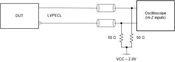
 Figure 8-7 LVPECL Output DC Test
Configuration
 Figure 8-8 LVPECL Output Phase Noise Test
Configuration
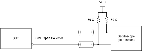
 Figure 8-9 CML Open
Collector Output DC Test Configuration
 Figure 8-10 CML Open
Collector Output Phase Noise Test Configuration
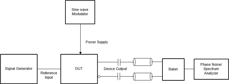
Single-sideband
spur level measured in dBc with a known noise amplitude and frequency injected
onto the device power supply.
Figure 8-11 Power
Supply Noise Rejection (PSNR) Test Configuration