ZHCSOB1A october 2021 – june 2023 LMK1D1208P
PRODUCTION DATA
9.4.2 Input Termination
The LMK1D1208P inputs can be interfaced with LVDS, LVPECL, HCSL, or LVCMOS drivers.
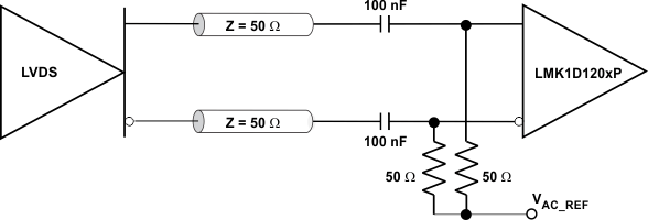
LVDS drivers can be connected to LMK1D1208P inputs with DC and AC coupling as shown Figure 9-3 and Figure 9-4, respectively.
 Figure 9-3 LVDS Clock Driver Connected to LMK1D1208P Input (DC-Coupled)
 Figure 9-4 LVDS Clock Driver Connected to LMK1D1208P Input (AC-Coupled)
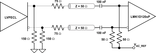
Figure 9-5 shows how to connect LVPECL inputs to the LMK1D1208P. The series resistors are required to reduce the LVPECL signal swing if the signal swing is >1.6 VPP.
 Figure 9-5 LVPECL Clock Driver Connected to LMK1D1208P Input
Figure 9-6 shows how to couple a LVCMOS clock input to the LMK1D1208P directly.
 Figure 9-6 1.8-V, 2.5-V, or 3.3-V
LVCMOS Clock Driver Connected to LMK1D1208P Input
Figure 9-6 1.8-V, 2.5-V, or 3.3-V
LVCMOS Clock Driver Connected to LMK1D1208P InputFor unused input, TI recommends grounding both input pins (INP, INN) using 1-kΩ resistors.