ZHCS747D January   2012  – September 2021 LMK01801

PRODUCTION DATA  

  1. 特性
  2. 应用
  3. 说明
  4. Revision History
  5. Device Comparison
    1. 5.1 Functional Configurations
  6. Pin Configuration and Functions
  7. Specifications
    1. 7.1 Absolute Maximum Ratings
    2. 7.2 Recommended Operating Conditions
    3. 7.3 Thermal Information
    4. 7.4 Electrical Characteristics
    5. 7.5 Serial MICROWIRE Timing Diagram
    6. 7.6 Typical Characteristics
  8. Parameter Measurement Information
    1. 8.1 Differential Voltage Measurement Terminology
  9. Detailed Description
    1. 9.1 Overview
    2. 9.2 Functional Block Diagram
    3. 9.3 Feature Description
      1. 9.3.1  High-Speed Clock Inputs (CLKin0/CLKin0* and CLKin1/CLKin1*)
      2. 9.3.2  Clock Distribution
      3. 9.3.3  Small Divider (1 to 8)
      4. 9.3.4  Large Divider (1 to 1045)
      5. 9.3.5  CLKout Analog Delay
      6. 9.3.6  CLKout0 to CLKout11 Digital Delay
      7. 9.3.7  CLKout12 and CLKout13 Digital Delay
      8. 9.3.8  Programmable Outputs
      9. 9.3.9  Clock Output Synchronization
      10. 9.3.10 Default Clock Outputs
    4. 9.4 Device Functional Modes
      1. 9.4.1 Programmable Mode
      2. 9.4.2 Pin Control Mode
      3. 9.4.3 Inputs / Outputs
        1. 9.4.3.1 CLKin0 and CLKin1
      4. 9.4.4 Input and Output Dividers
      5. 9.4.5 Fixed Digital Delay
        1. 9.4.5.1 Fixed Digital Delay - Example
      6. 9.4.6 Clock Output Synchronization (SYNC)
        1. 9.4.6.1 Dynamically Programming Digital Delay
          1. 9.4.6.1.1 Relative Dynamic Digital Delay
          2. 9.4.6.1.2 Relative Dynamic Digital Delay - Example
    5. 9.5 Programming
      1. 9.5.1 Recommended Programming Sequence
        1. 9.5.1.1 Overview
    6. 9.6 Register Map
      1. 9.6.1 Default Device Register Settings After Power On/Reset
      2. 9.6.2 Register R0
        1. 9.6.2.1 RESET
        2. 9.6.2.2 POWERDOWN
        3. 9.6.2.3 CLKoutX_Y_PD
          1. 9.6.2.3.1 CLKinX_BUF_TYPE
          2. 9.6.2.3.2 CLKinX_DIV
          3. 9.6.2.3.3 CLKinX_MUX
      3. 9.6.3 Register R1 and R2
        1. 9.6.3.1 CLKoutX_TYPE
      4. 9.6.4 Register R3
        1. 9.6.4.1 CLKout12_13_ADLY
        2. 9.6.4.2 CLKout12_13_HS, Digital Delay Half Shift
        3. 9.6.4.3 SYNC1_QUAL
        4. 9.6.4.4 SYNCX_POL_INV
        5. 9.6.4.5 NO_SYNC_CLKoutX_Y
        6. 9.6.4.6 CLKoutX_Y_OFFSET_PD
        7. 9.6.4.7 SYNCX_FAST
        8. 9.6.4.8 SYNCX_AUTO
      5. 9.6.5 Register R4
        1. 9.6.5.1 CLKout12_13_DDLY, Clock Channel Digital Delay
      6. 9.6.6 Register R5
        1. 9.6.6.1 CLKout12_ADLY_SEL[13], CLKout13_ADLY_SEL[14], Select Analog Delay
        2. 9.6.6.2 CLKoutX_Y_DIV Clock Output Divide
      7. 9.6.7 Register 15
        1. 9.6.7.1 uWireLock
  10. 10Application and Implementation
    1. 10.1 Typical Application
      1. 10.1.1 Detailed Design Procedure
        1. 10.1.1.1 Driving CLKin Inputs
          1. 10.1.1.1.1 Driving CLKin Pins With a Differential Source
          2. 10.1.1.1.2 Driving CLKin Pins With a Single-Ended Source
        2. 10.1.1.2 Termination and Use of Clock Output (Drivers)
          1. 10.1.1.2.1 Termination for DC-Coupled Differential Operation
          2. 10.1.1.2.2 Termination for AC-Coupled Differential Operation
          3. 10.1.1.2.3 Termination for Single-Ended Operation
  11. 11Power Supply Recommendations
    1. 11.1 Current Consumption
  12. 12Layout
    1. 12.1 Layout Guidelines
      1. 12.1.1 Pin Connection Recommendations
        1. 12.1.1.1 Vcc Pins and Decoupling
        2. 12.1.1.2 Unused clock outputs
        3. 12.1.1.3 Unused clock inputs
        4. 12.1.1.4 Unused GPIO (CLKoutTYPE_X)
        5. 12.1.1.5 Bias
        6. 12.1.1.6 In MICROWIRE Mode
    2. 12.2 Thermal Management
  13. 13Device and Documentation Support
    1. 13.1 Documentation Support
    2. 13.2 接收文档更新通知
    3. 13.3 支持资源
    4. 13.4 Trademarks
    5. 13.5 Electrostatic Discharge Caution
    6. 13.6 术语表
  14. 14Mechanical, Packaging, and Orderable Information

封装选项

机械数据 (封装 | 引脚)
散热焊盘机械数据 (封装 | 引脚)
订购信息
Driving CLKin Pins With a Single-Ended Source

The CLKin pins of the LMK01801 family can be driven using a single-ended reference clock source, for example, either a sine wave source or an LVCMOS/LVTTL source. Either AC coupling or DC coupling may be used. In the case of the sine wave source that is expecting a 50 Ω load, it is recommended that AC coupling be used as shown in Figure 10-4 the circuit below with a 50 Ω termination.

Note:

The signal level must conform to the requirements for the CLKin pins listed in the Section 7.4. CLKinX_BUF_TYPE is recommended to be set to bipolar mode (CLKinX_BUF_TYPE = 0).
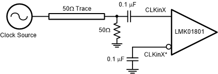
GUID-F9FE7E86-11CF-4FD9-8B6E-C7C137F8E148-low.gifFigure 10-4 DC-Coupled LVCMOS/LVTTL Reference Clock

If the CLKin pins are being driven with a single-ended LVCMOS/ LVTTL source, either DC coupling or AC coupling may be used. If DC coupling is used, see Figure 10-5, the CLKinX_BUF_TYPE should be set to MOS buffer mode (CLKinX_BUF_TYPE = 1) and the voltage swing of the source must meet the specifications for DC coupled, MOS-mode clock inputs given in the table of Electrical Characteristics. If AC coupling is used, the CLKinX_BUF_TYPE should be set to the bipolar buffer mode (CLKinX_BUF_TYPE = 0). The voltage swing at the input pins must meet the specifications for AC coupled, bipolar mode clock inputs given in the table of Electrical Characteristics. In this case, some attenuation of the clock input level may be required. A simple resistive divider circuit before the AC coupling capacitor is sufficient.

GUID-C954A783-44CD-4F67-B05B-306F83D5608C-low.pngFigure 10-5 DC-Coupled LVCMOS/LVTTL Reference Clock