ZHCS747D January 2012 – September 2021 LMK01801
PRODUCTION DATA
- 1 特性
- 2 应用
- 3 说明
- 4 Revision History
- 5 Device Comparison
- 6 Pin Configuration and Functions
- 7 Specifications
- 8 Parameter Measurement Information
-
9 Detailed Description
- 9.1 Overview
- 9.2 Functional Block Diagram
- 9.3
Feature Description
- 9.3.1 High-Speed Clock Inputs (CLKin0/CLKin0* and CLKin1/CLKin1*)
- 9.3.2 Clock Distribution
- 9.3.3 Small Divider (1 to 8)
- 9.3.4 Large Divider (1 to 1045)
- 9.3.5 CLKout Analog Delay
- 9.3.6 CLKout0 to CLKout11 Digital Delay
- 9.3.7 CLKout12 and CLKout13 Digital Delay
- 9.3.8 Programmable Outputs
- 9.3.9 Clock Output Synchronization
- 9.3.10 Default Clock Outputs
- 9.4 Device Functional Modes
- 9.5 Programming
- 9.6 Register Map
- 10Application and Implementation
- 11Power Supply Recommendations
- 12Layout
- 13Device and Documentation Support
- 14Mechanical, Packaging, and Orderable Information
10.1.1.2.2 Termination for AC-Coupled Differential Operation
AC coupling allows for shifting the DC bias level (common-mode voltage) when driving different receiver standards. AC coupling prevents the driver from providing a DC bias voltage at the receiver, therefore it is important to ensure the receiver is biased to its ideal DC level.
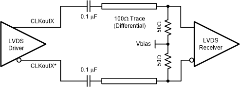
When driving non-biased LVDS receivers with an LVDS driver, the signal may be AC coupled by adding DC blocking capacitors, however the proper DC bias point needs to be established at the receiver. One way to do this is with the termination circuitry in Figure 10-9.
 Figure 10-9 Differential LVDS Operation, AC Coupling, External Biasing at the Receiver
Some LVDS receivers may have internal biasing on the inputs. In this case, the circuit shown in is modified by replacing the 50-Ω terminations to Vbias with a single 100-Ω resistor across the input pins of the receiver, as shown in Figure 10-10. When using AC coupling with LVDS outputs, there may be a start-up delay observed in the clock output due to capacitor charging. The previous figures employ a 0.1-μF capacitor. This value may need to be adjusted to meet the start-up requirements for a particular application.
 Figure 10-10 LVDS Termination for a Self-Biased Receiver
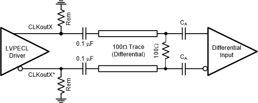
LVPECL drivers require a DC path to ground. When AC coupling an LVPECL signal use 120-Ω to 240-Ω emitter resistors close to the LVPECL driver to provide a DC path to ground as shown in Figure 10-11. For proper receiver operation, the signal should be biased to the DC bias level (common-mode voltage) specified by the receiver. The typical DC bias voltage for LVPECL receivers is 2 V.
A typical application is shown in Figure 10-11, where Rem = 120 Ω to 240 Ω. Refer to the receiver input recommendations to determine if the proper value of CA’s, if needed.
 Figure 10-11 Differential LVPECL Operation, AC Coupling,
External Biasing at the Receiver, Rem = 120 Ω to 240 Ω