SNOSB21D May 2008 – September 2016 LMH6518
PRODUCTION DATA.
- 1 Features
- 2 Applications
- 3 Description
- 4 Revision History
- 5 Pin Configuration and Functions
- 6 Specifications
- 7 Detailed Description
- 8 Application and Implementation
- 9 Power Supply Recommendations
- 10Layout
- 11Device and Documentation Support
- 12Mechanical, Packaging, and Orderable Information
8 Application and Implementation
NOTE
Information in the following applications sections is not part of the TI component specification, and TI does not warrant its accuracy or completeness. TI’s customers are responsible for determining suitability of components for their purposes. Customers should validate and test their design implementation to confirm system functionality.
8.1 Application Information
The LMH6518 device is ideal in applications that require a differential signal path and drive a differential, high-bandwidth analog to digital converter. The LMH6581 has 900 MHz of bandwidth and drives signals up to 1.8 VPP.
Typical applications for the LMH6518 include an oscilloscope AFE, gain control in a radio receiver, and a data acquisition system.
8.2 Typical Application
8.2.1 Oscilloscope Front End
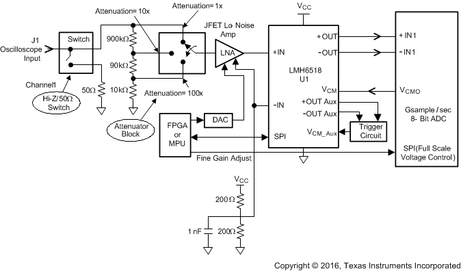 Figure 58. Digital Oscilloscope Front-End
8.2.1.1 Design Requirements
An oscilloscope is used to sample signals from millivolts to volts. To make the best use of the limited ADC input range, the oscilloscope input circuitry must have a wide gain range.
In this design example, the LMH6518 is driving an ADC12J2700 and has the following requirements:
- Common mode voltage = 1.225 V
- Full scale voltage = 650 mVPP to 800 mVPP
- Bandwidth = 900 MHz
- Trigger channel
- Spurious free dynamic range = 50 dB
8.2.1.2 Detailed Design Procedure
Figure 59 shows a block diagram of the LMH6518's main output signal path.
 Figure 59. LMH6518 Signal Path Block Diagram
The auxiliary output (not shown) uses another but similar output amplifier that taps into the ladder attenuator output. In this data sheet, preamp gain of 30 dB is referred to as high gain (HG), and preamp gain of 10 dB as low gain (LG).
The LMH6518 2-dB/step gain resolution and 40-dB adjustment range (from −1.16 dB to 38.8 dB) allows this device to be used with the TI Gsps ADCs which have full scale (FS) adjustment through their extended control mode (ECM) to provide near-continuous variability (8.5-mdB resolution) which covers 42.6 dB FS input range using Equation 1.

TI's Gsps ECM control allows the ADC FS to be set using the ADC SPI bus. The ADC FS voltage range is from 560 mV to 840 mV with 9 bits of FS voltage control.
The ADC ECM gain resolution is calculated with Equation 2.

However, the recommended ADC FS operating range is narrower; it is from 595 mV to 805 mV with 700 mVPP as the mid-point. Raising the value of ADC FS voltage is tantamount to reducing the signal path gain to accommodate a larger input and vice versa, thus providing a method of gain fine-adjust. The ADC ECM gain adjustment is −1.21 dB as in Equation 3.

Because the ADC FS fine-adjust range of 2.62 dB (= 1.41 dB + 1.21 dB) is larger than the LMH6518’s 2-dB/step resolution, there is always at least one LMH6518 gain setting to accommodate any FS signal from 6.8 mVPP to 920 mVPP, at the LMH6518 input, with 0.62 dB (= 2.62-2) overlap.
Assuming a nominal 0.7-VPP output, the LMH6518’s minimum FS input swing is limited by the maximum signal path gain possible and vice versa with Equation 4.

(or 8 mVPP with no ADC fine adjust in Equation 5)

(or 800 mVPP with no ADC FS adjust)
To accommodate a higher FS input, an additional attenuator is required before the LMH6518. This front-end attenuator is shown in the Figure 58 with its details shown in Figure 69. The highest minimum attenuation level is determined by the largest FS input signal (FSmax) in Equation 6.

So, to accommodate 80 VPP, 40 dB minimum attenuation is required before the LMH6518.
In a typical oscilloscope application, the voltage range encountered is from 1 mV/DIV to 10 V/DIV with 8 vertical divisions visible on the screen. One of the primary concerns in a digital oscilloscope is SNR which translates to display trace width to thickness. Typically, oscilloscope manufacturers require the noise level to be low enough so that the no-input visible trace width is less than 1% of FS. Experience shows that this corresponds to a minimum SNR of 52 dB.
The factors that influence SNR are:
- Scope front end noise (Front-end attenuator + scope probe Hi-Z buffer which is discussed later in this data sheet and shown in Figure 58)
- LMH6518
- ADC
LMH6518 related SNR factors are:
- Bandwidth
- Preamp used (Preamp HG or LG)
- Ladder attenuation
- Signal level
SNR increases with the inverse square root of the bandwidth. So, reducing bandwidth from 450 MHz to
200 MHz, for example, improves SNR by 3.5 dB as seen in Equation 7.

The other factors listed above, preamp and ladder attenuation, depend on the signal level and also impact SNR. The combined effect of these factors is summarized in Figure 60, where SNR is plotted as a function of the LMH6518 FS input voltage (assuming scope bandwidth of 200 MHz) and not including the ADC and the front end noise.
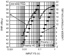 Figure 60. LMH6518 SNR and Ladder Attenuation Used vs Input
As seen in Figure 60, SNR of at least 52 dB is maintained for FS inputs above 24 mVPP (3 mV/DIV on a scope) assuming the LMH6518’s internal 200 MHz filter is enabled. Most oscilloscope manufacturers relax the SNR specifications to 40 dB for the highest gain (lowest scope voltage setting). From Figure 60, LMH6518’s minimum SNR is 43.5 dB, thereby meeting the relaxed SNR specification for the lower range of scope front panel voltages.
In Figure 60, the step-change in SNR near Input FS of 90 mVPP is the transition point from preamp LG to preamp HG with a subsequent 3 dB difference due to the preamp HG to 20-dB ladder attenuation’s lower output noise compared to preamp LG to 2-dB ladder attenuation’s noise. Judicious choice of front-end attenuators ensures that the 52-dB SNR specification is maintained for scope FS inputs ≥24 mVPP by confining the LMH6518 gain range to the lower 30.5 dB using Equation 8 from the total range of 40 dB (= 38.8 – (−1.16)) is possible.

For example, to cover the range of 1 mV/DIV to 10 V/DIV (80 dB range), Table 5 lists a configuration which affords good SNR.
Table 5. Oscilloscope Example Including Front-End Attenuators
| ROW | SCOPE FS INPUT (VPP) | S, SCOPE VERTICAL SCALE (V/DIV) | PREAMP | LADDER ATTENUATION RANGE (dB) | A, FRONT-END ATTENUATION (V/V) | MINIMUM SNR (dB) WITH 200 MHz FILTER |
|---|---|---|---|---|---|---|
| 1 | 8 m to 24 m | 1 m to 3 m | HG | 0 to 10 | 1 | 44 |
| 2 | 24 m to 80 m | 3 m to 10 m | HG | 10 to 20 | 1 | 52 |
| 3 | 80 m to 0.8 | 10 m to 0.1 | LG | 0 to 20 | 1 | 53.4 |
| 4 | 0.8 to 8 | 0.1 to 1 | LG | 0 to 20 | 10 | 53.4 |
| 5 | 8 to 80 | 1 to 10 | LG | 0 to 20 | 100 | 53.4 |
In Table 5, the highest FS input in row 5, column 2 (80 VPP), and the LMH6518’s highest FS input allowed
(0.8 VPP) set the front-end attenuator value with Equation 9.

The 100x attenuator allows high-SNR operation to 30.5 dB down, as explained earlier, or 2.4 VPP at scope input. In that same table, rows 1 to 3 with no front-end attenuation (1x) cover the scope FS input range from 8 mVPP to 800 mVPP. That leaves the scope FS input range of 0.8 VPP to 2.4 VPP. If the 100x attenuator were used for the entire scope FS range of 0.8 VPP to 80 VPP, SNR would dip below 52 dB for a portion of that range. Another attenuation level is thus required to maintain the SNR specification requirement of 52 dB.
One possible attenuation partitioning is to select the additional attenuator value to cover a 20 dB range above
0.8 VPP FS (to 8 VPP) with the 100x attenuator covering the remaining 20 dB range from 8 VPP to 80 VPP. Mapping 8 VPP FS scope input to 0.8 VPP at LMH6518 input means the additional attenuator is 10x, as shown in Table 5, row 4. The remaining scope input range of 8 VPP to 80 VPP is then covered by the 100x front-end attenuator derived earlier. The entire scope input range is now covered with SNR maintained about 52 dB for scope FS input ≥24 mVPP, as shown in Table 5.
8.2.1.2.1 Settings and ADC SPI Code (ECM)
Covering the range from 1 mV/DIV to 10 V/DIV requires the following adjustment within the digital oscilloscope:
- Front-end attenuator
- LMH6518 preamp
- LMH6518 ladder attenuation
- ADC FS value (ECM)
The LMH6518 product folder contains a spreadsheet which allows one to calculate the front-end attenuator, LMH6518 preamp gain (HG or LG), ladder attenuation, and ADC FS setting based on the scope vertical scale
(S in V/DIV).
Here is the step-by-step procedure that explains the operations performed by the said spreadsheet based on the scope vertical scale setting (S in V/div) and front-end attenuation A (from Table 5). A numerical example is also worked out for more clarification:
- Determine the required signal path gain, K, with Equation 10:
- Determine the LMH6518 gain, G:
- G is the closest LMH6518 gain, to the value of K where:
- G = (38.8 – 2n)dB; n = 0, 1, 2, …, 20
- For this example, the closest G to K = 17.57 dB is 16.8 dB (with n = 11). The next LMH6518 gain,
18.8 dB (with n = 10) is incorrect as 16.8 is closer. If 18.8 dB were mistakenly chosen, the ADC FS setting is out of range. - Therefore: G = 16.8 dB
- Determine preamp (HG or LG) and ladder attenuation:
- If G ≥ 18.8 dB → Preamp is HG and ladder attenuation = 38.8 – G
- If G < 18.8 dB → Preamp is LG and ladder attenuation = 18.8 – G
- For this example, with G = 16.8 → Preamp LG and Ladder Attenuation = 2 dB (= 18.8 to 16.8).
- Determine the required ADC FS voltage, FSE, with Equation 12:
- Determine the ADC ECM code ratio with Equation 14:
- 0.28 V = (0.84 – 0.56) V
- 0.56 V is the lower end of the ADC FS adjustability
- For this example:
- Required condition: 0 ≤ ECM (ratio) ≤ 1
Equation 14.
where

- Determine the ECM binary code sent on ADC SPI bus:
- Convert the ECM value represented by the ratio calculated above, to binary:
- ECM (binary) = DEC2BIN{ECM(ratio) × 511, 9}
- Where DEC2BIN is a spreadsheet function which converts the decimal ECM ratio, from step 5 above, multiplied by 511 distinct levels, into binary 9 bits.
- For this example: ECM (binary) = DEC2BIN(0.283 × 511, 9) = 010010000. This is the number sent to the ADC on the SPI bus to program the ADC to proper FS voltage.
NOTE
The Web based spreadsheet computes ECM without the use of DEC2BIN function to ease usage by all spreadsheet users who may not have this function installed.

(assuming the full scale signal occupies 95% of the 0.7 VPP FS for 5% overhead which occupies 8 vertical scope divisions).
Required condition: −2.37 dB ≤ K ≤ 40.3 dB
Example: With S = 110 mV/DIV, Table 5 shows that A = 10 V/V in Equation 11.


The 1.05 factor is to add 5% FS overhead margin to avoid ADC overdrive with Equation 13.

Required condition: 0.56 V ≤ FSE ≤ 0.84 V
Recommend condition: 0.595 V ≤ FSE ≤ 0.805 V for optimum ADC FS
8.2.1.2.2 Input and Output Considerations
The LMH6518’s ideal input and output conditions, considered individually, are listed in Table 6.
Table 6. LMH6518's Ideal Input and Output Conditions
| IMPEDANCE FROM EACH INPUT TO GROUND (Ω) | COMMON MODE INPUT (V) | DIFFERENTIAL INPUT (VPP) | LOAD IMPEDANCE (Ω) | DIFFERENTIAL OUTPUT (V) | COMMON MODE OUTPUT (V) |
|---|---|---|---|---|---|
| ≤50 | 1.5 to 3.1 | <0.8 | 100 (differential) and 50 (single-ended) |
<0.77 | 0.95 to 1.45 |
In addition to the individual conditions listed in Table 6, the input and output terminal conditions must match differentially (that is, +IN to −IN and +OUT to −OUT), as well, for best performance.
The input is differential but is driven single-ended as long as the conditions of Table 6 are met, and there is good matching between the driven and undriven inputs from DC to the highest frequency of interest. If not, there is a settling time impact among other possible performance degradations. The data sheet specifications are with single-ended input, unless specified. Figure 61 is the recommended bench-test schematic to drive one input and to bias the other input with good matching in mind.
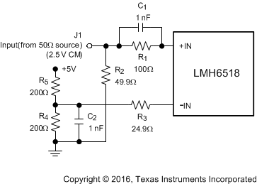 Figure 61. Recommended Single-Ended Bench-Test Input Drive from 50-Ω Source
With Figure 61, each LMH6518 input sees 25 Ω to ground at higher frequencies when the capacitors look like shorts. This impedance increases to 125 Ω at DC for both inputs, thereby preserving the required matching at any frequency. This configuration, using properly selected R’s and C’s, allows four times less biasing power dissipation than when undriven inputs are biased with an effective 25 Ω from the LMH6518 input to ground.
It is possible to drive the LMH6518 input from a ground-referenced, 50-Ω source by providing level shift circuitry on the driven input. Figure 62 shows a circuit where half the input signal reaches the LMH6518 input while the negative supply voltage (VEE) ensures that the 50Ω source at J1 does not experience any biasing current while providing 50-Ω termination to the source. The driven input (+IN) is biased to 2.5 V (VCC/2) in Figure 62.
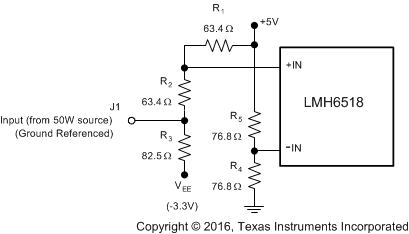 Figure 62. LMH6518 Driven by a Ground Referenced Source
In Figure 62, the equivalent impedance from each LMH6518 input to ground is around 38 Ω. The power consumption of this configuration is approximately 0.5 W (in R1 – R5) which is higher than that of Figure 61 because of additional power dissipated to perform the level shifting. Additional 50-Ω attenuators is placed between J1 and R2/R3 junction in Figure 62 to accommodate higher input voltages.
It is also possible to shift the LMH6518 output common mode level using a level shift approach similar to that of Figure 62. The circuit in Figure 63 shows an implementation where the LMH6518’s nominal 1.2 V CM output, set by a 1.2 V on VCM input from the Gsps ADC, is shifted lower for proper interface to different ADCs (which require VCM = 0 V and have high input impedance).
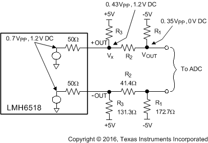 Figure 63. Output CM Shift Scheme
In Figure 63, Vx is kept at 1.2 V by proper selection of external resistor values, so that the LMH6518 outputs are not CM-loaded. As was the case with input level shifting, this output-level shifting also consumes additional power (0.58 W).
8.2.1.2.2.1 Output Swing, Clamping, and Operation Beyond Full Scale
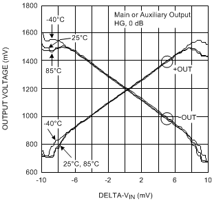
One of the major concerns in interfacing to low voltage ADC’s (such as the Gsps ADC that the LMH6518 is intended to drive) is ensuring that the ADC input is not violated with excessive drive. For this reason, plus the important requirement of an oscilloscope to recover quickly and gracefully from an overdrive condition, the LMH6518 is fitted with three overvoltage clamps; one at the preamp output, and one at the main and auxiliary outputs (each). The preamp clamp is responsible for preventing the preamp from saturation (to minimize recovery time) with large ladder attenuation when preamp output swing is at its highest. On the other hand, the output clamps perform this function when ladder attenuation is lower. Therefore, the output amplifier is closer to saturation and prolonged recovery (if not properly clamped). The combination of these clamps results in Figure 50, Figure 51, Figure 52, and Figure 66. With these four graphs, it is possible to observe where output limiting starts due to the clamp action. LMH6518 owes its fast recovery time (<5 ns) from 50% overdrive to the said clamps.
Figure 50, Figure 51, Figure 52, and Figure 66 in Typical Characteristics is used to determine the LMH6518 linear swing beyond full scale. This information sets the overdrive limit for both oscilloscope waveform capture and signal triggering. The preamp clamp is set tighter than the output clamp, evidenced by lower output swing with 20-dB ladder attenuation than with 0 dB. With high ladder attenuation (20 dB) defining the limit, the graphs show that the +OUT and −OUT difference of 0.4 V is well inside the clamp range, thereby ensuring 0.8 VPP of unhindered output swing. This corresponds to an overdrive capability of approximately ±7% beyond full scale.
From Figure 58, the signal path consists of the input impedance switch, the attenuator switch, low noise amplifier (LNA, JFET amplifier) to drive the LMH6518 input (+IN), and the DAC to provide offset adjust. The LNA must have the following characteristics:
- Set U1’s common mode level to VCC/2 (approximately 2.5 V)
- Low drift (1 mV shift at LNA output could translate into 88 mV shift at LMH6518 output at maximum gain, or approximately 13% of FS)
- Low output impedance (≤ 50 Ω) to drive U1 for good settling behavior
- Low noise (<0.98 nV/√Hz) to reduce the impact on the LMH6518 noise figure. Note that Figure 58 does not show the necessary capacitors across the resistors in the front-end attenuators (see Figure 69). These capacitors provide frequency response compensation and limit the noise contribution from the resistors so that they do not impact the signal path noise. For more information about front-end attenuator design, including frequency compensation, see Related Documentation for additional resources.
- Gain of 1 V/V (or close to 1 V/V)
- Excellent frequency response flatness from DC to >500 MHz to 800 MHz to not impact the time domain performance
The undriven input (−IN) is biased to VCC/2 using a voltage driver. The impedance driving the LMH6518’s −IN must be closely matched to the LNA’s output impedance for good settling time performance.
JFET LNA Implementation shows one possible implementation of the LNA buffer along with performance data.
When the LMH6518’s auxiliary output is not used, it is possible to disable this output using SPI-1 (see Logic Functions for SPI register map). Electrical Characteristics shows that by doing so, device power dissipation decreases by the reduction in supply current of about 60 mA. As seen in Figure 64, in the absence of heavy common loading, the auxiliary output is at a voltage close to 1.7 V (VCC = 5 V). With higher supply voltages, the auxiliary voltage also increases. It is important to ensure any circuitry tied to this output is capable of handling the 2.3 V possible under VCC worst case condition of 5.5 V.
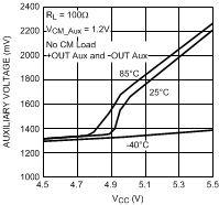 Figure 64. Auxiliary Output Voltage as a Function of VCC
8.2.1.2.3 Oscilloscope Trigger Applications
With the Auxiliary output of the LMH6518 offering a second output that follows the main one (except for a slightly reduced distortion performance), the oscilloscope trigger function is implemented by tapping this output. The auxiliary common mode is set with the VCM_Aux input of the LMH6518. If required, the trigger function is placed at a distance from the main signal path by taking advantage of the differential auxiliary output and rejecting any board related common mode interference pick-up at the receive end.
If trigger circuitry is physically close to the LMH6518, the circuit diagram shown in Figure 65 allows operation using only one of two auxiliary outputs. Unused outputs require proper termination using R1, R11 combination. U3 (DAC101C085) generates a 0- 2.5 V trigger level, with 2.4 mV resolution as in Equation 15 or 0.7%
(= 2.4 mV × 100/0.35 VPP) of FS, which is compared to the LMH6518 +OUT AUX by using an ultra-fast comparator, U2 (LMH7220). U2’s complimentary LVDS output is terminated in the required 100-Ω load (R10), for best performance, where the LVDS trigger output is available.

The LMH7220’s offset voltage (±9.5 mV) and offset voltage drift (±50 µV/°C) error is 5.9 LSB of the trigger DAC (U3) as in Equation 16.

The offset voltage related portion of this error is nulled-out, if necessary, during the oscilloscope initial calibration. To do so, the LMH6518 input is terminated properly with no input applied and U3 output is adjusted around VCM_Aux voltage (1.2 V ±10 mV) while looking for U2’s output transition. U3’s output, relative to VCM_Aux at transition corresponds to U2’s offset error which is factored into the trigger readings and thus eliminated, leaving only the offset voltage temperature drift component (= 2 LSB).
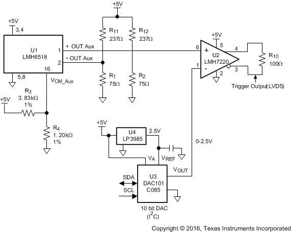 Figure 65. Single-Ended Trigger from LMH6518 Auxiliary Output
U2’s minimum toggle rate specification of 750 Mb/s with ±50 mV overdrive allow the oscilloscope to trigger on repetitive waveforms well above the 500 MHz oscilloscope bandwidth applications, when the input signal is at least 14.3% of FS swing with Equation 17.

The worst case single event minimum discernable pulse width is set by the LMH7220’s propagation delay specification of 3.63 ns (20 mV overdrive).
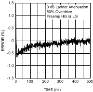
Both the main and the auxiliary outputs recover gracefully and quickly from a 50% overdrive condition as tabulated in Electrical Characteristics under overdrive recovery time. However, overdrive conditions beyond 50% could result in longer recovery times due to the interaction between an internal clamp and the common mode feedback loop that sets the output common mode voltage. This may have an impact on both the displayed waveform and the oscilloscope trigger. The result is a loss of trigger pulse or visual distortion of the displayed waveform. To avoid this scenario, the oscilloscope must detect an excessive overdrive and go into trigger-loss mode. Done this way, the oscilloscope display would show the last waveform that did not violate the overdrive condition. Preferably, there is a visual indicator on the screen that alerts the user of the excessive condition, and returns the display to normal once the condition is corrected.
8.2.2 JFET LNA Implementation
Figure 68 shows the schematic drawing for a possible implementation of the LNA buffer.
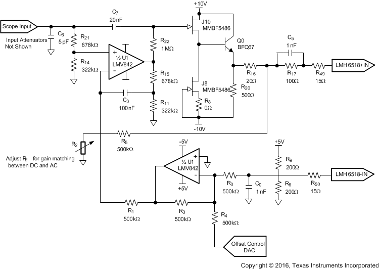 Figure 68. JFET LNA Implementation
8.2.2.1 Design Requirements
This circuit uses an N-Channel JFET (J10) in source-follower configuration to buffer the input signal with J8 acting as a constant current source. This buffer presents a fixed input impedance (1 MΩ||10 pF) with a gain close to 1 V/V.
The signal path is AC-coupled through C7 with DC (and low frequency) at LMH6518 +IN maintained through the action of U1. NPN transistor Q0 is an emitter follower which isolates the buffer from the load (LMH6518 input and board traces).
The undriven input of the LMH6518 (−IN) is biased to 2.5 V by R6, R9 voltage divider. The lower half of U1 inverts this voltage and the upper half of U1 compares it to the combination of the driven output level at LMH6518 +IN and the scaled version of scope input at R14, R21 junction, and adjusts J10 Gate accordingly to set the LMH6518 +IN. This control loop has a frequency response that covers DC to a few Hz, limited by the roll-off capacitor C3 and R15 combination (first order approximation). DC and low frequency gain is given by Equation 18.

With the values in Figure 68 → R2 approximately 452 kΩ.
For a flat frequency response, the DC (low frequency) gain requires lowering to match the less-than-1 V/V AC (high frequency) path gain through the JFETs. This is done by increasing the value of R2.
Choose values of R15 and R11 so that the frequency response at J10 Gate (and consequently the output) remain flat when C7 starts to conduct as in Equation 19.

Offset correction is done by varying the voltage at R4, using a DAC or equivalent as shown, to shift the LMH6518 +IN voltage relative to −IN. The result is a circuit which shifts the ground referenced scope input to
2.5 V (VCC/2) CM with adjustable offset and without any JFET or BJT related offsets.
Note that the front-end attenuator (not shown) lower leg resistance is increased for proper divider-ratio to account for the 1-MΩ shunt due to the series combination of R21 and R14. For example, a 10:1 front-end attenuator is formed by a series 900 kΩ and a shunt 111 kΩ for a scope BNC input impedance of
1 MΩ (= 900 K + (111 K || 1 M)).
Table 7 lists other possible JFET candidates that fall in the range of speed (ft) and low noise requirement.
Table 7. Suitable JFET Candidates Specifications
| COMPANY | PART NUMBER | VP (V) | Idss (mA) | gm (mS) | INPUT C (pF) |
NOISE(1)
(nV/RtHz) |
BREAK DOWN (V) |
CALCULATED ft (MHz) |
|---|---|---|---|---|---|---|---|---|
| Interfet | IF140 | –2.2 | 10 | 5.5 | 2.3 | 4 | –20 | 380 |
| Interfet | IF142 | –2.2 | 10 | 5.5 | 2.3 | 4 | –25 | 380 |
| Interfet | 2N5397/8 | –2.5 | 13 | 8 | 5 | 2.5 | –25 | 254 |
| Interfet | 2N5911/2 | –2.5 | 13 | 8 | 5 | 2.5 | — | 254 |
| Interfet | J308/9/10 | –2.3 | 21 | 17 | 5.8 | — | –25 | 466 |
| Philips | BF513 | –3 | 15 | 10 | 5 | — | — | 318 |
| Fairchild | MMBF5486 | –4 | 14 | 7 | 4 | 2.5 | –25 | 278 |
| Vishay Siliconix | SST441 | –3.5 | 13 | 6 | 3.5 | 4 | –35 | 272 |
The LNA noise could degrade the scope’s SNR if it is comparable to the input referred noise of the LMH6518. LNA noise is influenced by the following operating conditions:
- JFET equivalent input noise
- BJT base current
Reducing either a or b above, or both, reduces noise. One way to reduce a is to increase R8 (currently set to
0 Ω). This reduces the noise impact of J8 but requires a JFET which has a higher Idss rating to maintain the operating current of J10 so that J10’s noise contribution is minimized. Reducing the BJT base current is accomplished with increasing R20 at the expenses of higher rise/fall times. A higher β also reduces the base current (keep in mind that β and ft at the operating collector current is what matters).
Figure 70 shows the impact of the JFET buffer noise on SNR, compared to SNR in Figure 60, assuming either
3 nV/√Hz or 1.5 nV/√Hz buffer noise for comparison.
8.2.2.2 Detailed Design Procedure
8.2.2.2.1 Attenuator Design
Figure 69 shows a front-end attenuator designed to work with Figure 68.
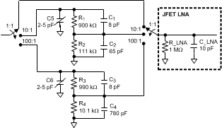 Figure 69. Front End Attenuator for JFET LNA Implementation
R_LNA and C_LNA are the input impedance components of the JFET LNA. The 10:1 and 100:1 attenuators bottom resistors (R2 and R4) are adjusted higher to compensate for the LNA’s 1-MΩ input impedance, compared to the case where a high-input-impedance LNA is used. The two switches used on the input and output of the attenuator block are low-capacitance, high-isolation switches to reduce any speed or crosstalk impact. C1 to C4 provide the proper frequency response (and step response) by creating zeros that flatten the response for wide-band operation. For the 10:1 attenuator, R1C1 = R2C2. The same applies to the 100:1 attenuator. The shunt capacitors, C1 to C4, have a important other benefit in that they roll-off the resistor thermal noise at a low frequency (low pass response, −3 dB down at approximately 20 kHz) thereby eliminating any significant noise contribution from the attenuation resistors. Otherwise, the channel noise is dominated by the attenuator resistor thermal noise. C2 and C6 trimmer capacitors are adjusted to match the input capacitance regardless of attenuator used.
8.2.2.3 Application Curve
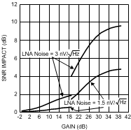 Figure 70. LNA Buffer SNR Impact
