at
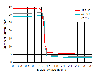
VDD = 3.3 V, VOCM = open, VOD = 0 V,
CPD = 1 pF, EN = 0 V (enabled),
IDC_EN = 3.3 V (disabled), RL = 100 Ω
(differential load between OUT+ and OUT–), and TA = 25°C (unless
otherwise noted)

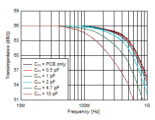
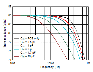
| Gain = 2 kΩ, VOUT = 100 mVPP
|
Figure 6-1 Small-Signal Response vs Input
Capacitance
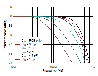
| Gain = 2 kΩ, VOUT = 1 VPP |
Figure 6-3 Large-Signal Response vs Input
Capacitance
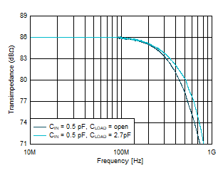
| Gain
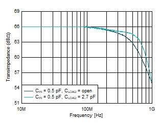
= 2 kΩ, VOUT = 100 mVPP |
Figure 6-5 Small-Signal Response vs Load
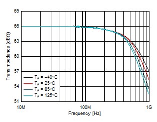
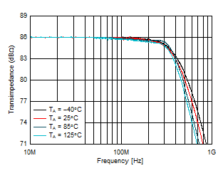
Capacitance Figure 6-7 Small-Signal Response vs Ambient
Temperature
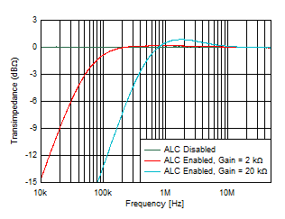
 Figure 6-9 Low-side Frequency Response vs
Ambient‑Light Cancellation
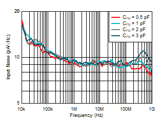
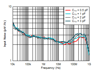
 Figure 6-11 Input Noise Density vs Input
Capacitance
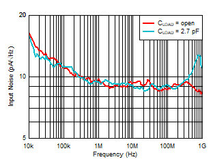
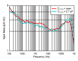
 Figure 6-13 Input Noise Density vs Load
Capacitance
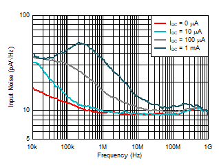
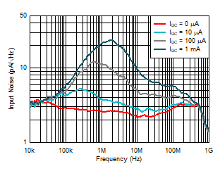
 Figure 6-15 Input Noise Density vs
Ambient-Light DC Current
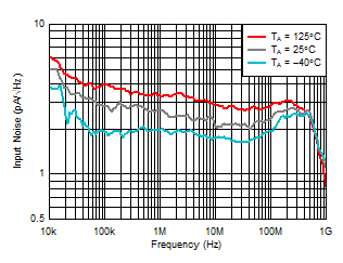
 Figure 6-17 Input Noise Density vs Ambient
Temperature
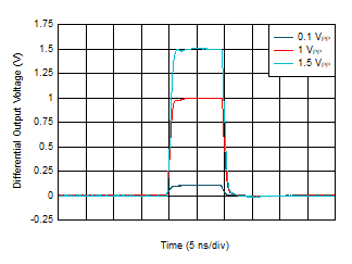
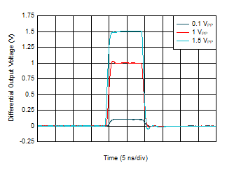
 Figure 6-19 Pulse Response vs Output
Swing
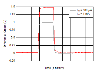
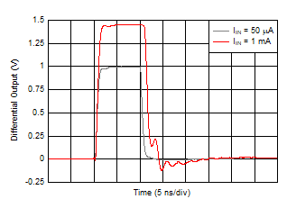
 Figure 6-21 Overloaded Pulse Response
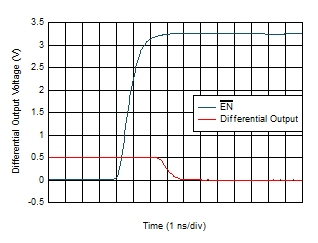
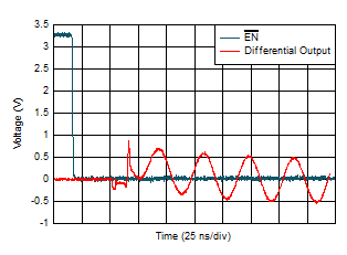
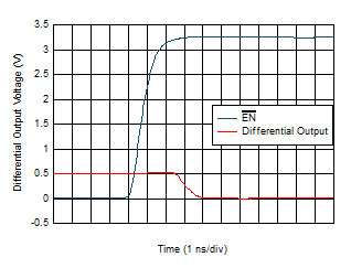
  Figure 6-23 Turn-On Time
| Gain
= 2 kΩ, VVOD = 0.5 V |
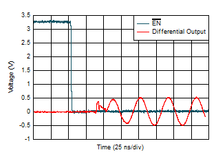
Figure 6-25 Turn-Off Time
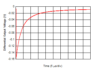
| Gain
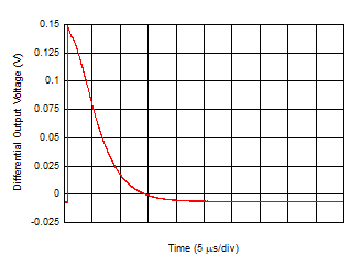
= 2 kΩ, IDC_IN = 0 µA → 100 µA (current due
to ambient light transitions at the lowest displayed
value of the time axis) |
Figure 6-27 Ambient Loop Cancellation Settling
Time
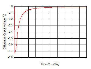
| Gain
= 20 kΩ, IDC_IN = 0 µA → 100 µA (current due
to ambient light transitions at the lowest displayed
value of the time axis) |
Figure 6-29 Ambient Loop-Cancellation Settling
Time
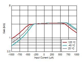
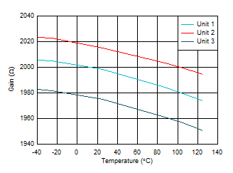
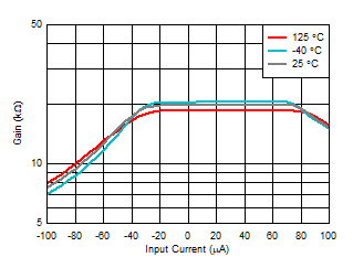
| Gain
= 2 kΩ, positive current is sinking current into the
photodiode cathode |
Figure 6-31 Transimpedance Gain vs Input
Current  Figure 6-33 Transimpedance Gain vs Ambient
Temperature
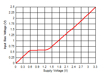
 Figure 6-35 Input Bias Voltage vs Supply
Voltage
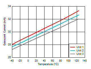
 Figure 6-37 Quiescent Current vs Ambient
Temperature
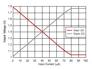
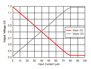
| VVOD = 0.75 V, VVOCM = 1.4
V |
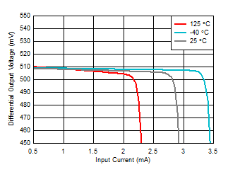
Figure 6-39 High-side Swing vs Input
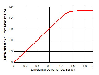
Current Figure 6-41 Differential Output Offset
Gain
| Logic switching demonstrated using
EN pin. |
| IDC_EN and gain pins behave
similarly. |
Figure 6-43 Logic Threshold vs Ambient
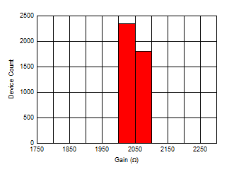
Temperature Figure 6-45 Transimpedance Gain (Low)
Distribution
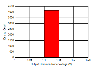
 Figure 6-47 Output Common-Mode Voltage
(VOCM) Distribution
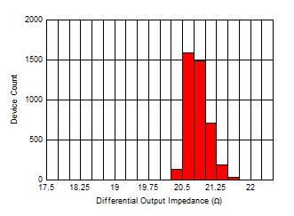
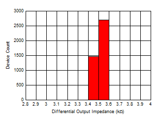
 Figure 6-49 Differential Output Impedance
(ZOUT) Distribution
| Gain = 20 kΩ, VOUT = 100 mVPP
|
Figure 6-2 Small-Signal Response vs Input
Capacitance
| Gain = 20 kΩ, VOUT = 1
VPP |
Figure 6-4 Large-Signal Response vs Input
Capacitance
| Gain
= 20 kΩ, VOUT = 100 mVPP |
Figure 6-6 Small-Signal Response vs Load
Capacitance Figure 6-8 Small-Signal Response vs Ambient
Temperature
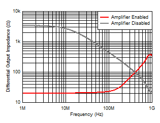
 Figure 6-10 Closed-Loop Output Impedance vs
Frequency
 Figure 6-12 Input Noise Density vs Input
Capacitance
 Figure 6-14 Input Noise Density vs Load
Capacitance
 Figure 6-16 Input Noise Density vs
Ambient-Light DC Current
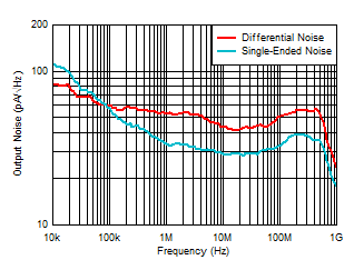
 Figure 6-18 Output Noise Density vs Output
Configuration
  Figure 6-20 Pulse Response vs Output
Swing
 Figure 6-22 Overloaded Pulse Response
  Figure 6-24 Turn-On Time
| Gain
= 20 kΩ, VVOD = 0.5 V |
Figure 6-26 Turn-Off Time
| Gain
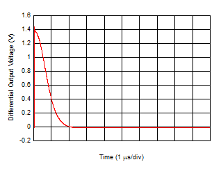
= 2 kΩ, IDC_IN = 100 µA → 0 µA (current due
to ambient light transitions at the lowest displayed
value of the time axis) |
Figure 6-28 Ambient Loop-Cancellation Settling
Time
| Gain
= 20 kΩ, IDC_IN = 100 µA → 0 µA (current due
to ambient light transitions at the lowest displayed
value of the time axis) |
Figure 6-30 Ambient Loop-Cancellation Settling
Time
| Gain
= 20 kΩ, positive current is sinking current into the
photodiode cathode |
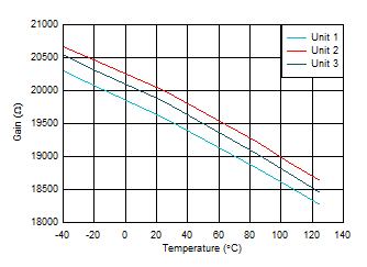
Figure 6-32 Transimpedance Gain vs Input
Current Figure 6-34 Transimpedance Gain vs Ambient
Temperature
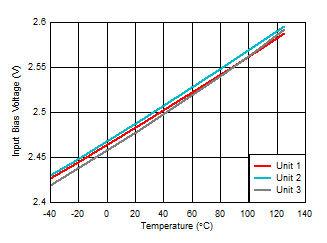
 Figure 6-36 Input Bias Voltage vs Ambient
Temperature
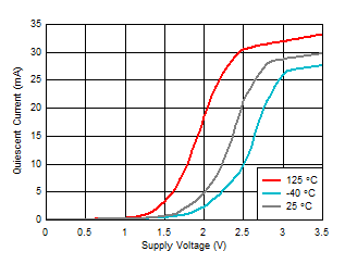
 Figure 6-38 Quiescent Current vs Supply
Voltage
| VVOD = 0.75 V, VVOCM = 0.8
V |
Figure 6-40 Low-side Swing vs Input
Current Figure 6-42 Ambient Light Cancellation Range vs
Ambient Temperature
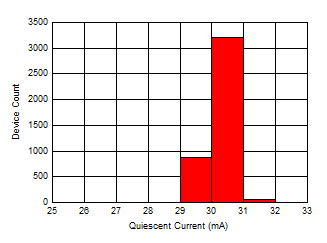
 Figure 6-44 Quiescent Current
Distribution
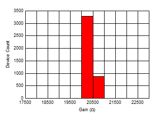
 Figure 6-46 Transimpedance Gain (High)
Distribution
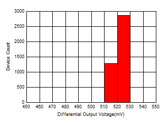
 Figure 6-48 Differential Output Offset Voltage
(VOD) Distribution
 Figure 6-50 Differential Output Impedance
(ZOUT) Distribution
