SNLS289D April   2008  – September 2015 LMH1982

PRODUCTION DATA.  

  1. Features
  2. Applications
  3. Description
  4. Revision History
  5. Pin Configuration and Functions
  6. Specifications
    1. 6.1 Absolute Maximum Ratings
    2. 6.2 ESD Ratings
    3. 6.3 Recommended Operating Conditions
    4. 6.4 Thermal Information
    5. 6.5 Electrical Characteristics
    6. 6.6 Typical Characteristics
  7. Detailed Description
    1. 7.1 Overview
    2. 7.2 Functional Block Diagram
    3. 7.3 Feature Description
      1. 7.3.1 Supported Standards and Timing Formats
    4. 7.4 Device Functional Modes
      1. 7.4.1 Modes of Operation
        1. 7.4.1.1 Free Run Mode
        2. 7.4.1.2 Genlock Mode
          1. 7.4.1.2.1 Genlock Mode State Diagram
            1. 7.4.1.2.1.1 Loss of Reference (LOR)
              1. 7.4.1.2.1.1.1 Free Run during LOR
              2. 7.4.1.2.1.1.2 Holdover during LOR
    5. 7.5 Programming
      1. 7.5.1 I2C Interface Protocol
        1. 7.5.1.1 Write Sequence
        2. 7.5.1.2 Read Sequence
        3. 7.5.1.3 I2C Enable Control Pin
    6. 7.6 Register Maps
      1. 7.6.1 I2C Interface Control Register Definitions
        1. 7.6.1.1 Genlock and Input Reference Control Registers
        2. 7.6.1.2 Genlock Status And Lock Control Register
        3. 7.6.1.3 Input Control Register
        4. 7.6.1.4 PLL 1 Divider Register
        5. 7.6.1.5 PLL 4 Charge Pump Current Control Register
        6. 7.6.1.6 Output Clock and TOF Control Register
        7. 7.6.1.7 TOF Configuration Registers
        8. 7.6.1.8 PLL 1, 2, 3 Charge Pump Current Control Registers
        9. 7.6.1.9 Reserved Registers
  8. Application and Implementation
    1. 8.1 Application Information
      1. 8.1.1 148.35 MHz PLL Initialization Sequence
      2. 8.1.2 Enabling Genlock Mode
      3. 8.1.3 Output Disturbance While Output Alignment Mode Enabled
      4. 8.1.4 Evaluating the LMH1982
      5. 8.1.5 Input Reference
        1. 8.1.5.1 Reference Frame Decoder
      6. 8.1.6 Output Clocks and TOF
        1. 8.1.6.1 Programming the Output Clock Frequencies
        2. 8.1.6.2 Programming the Output Format Timing
          1. 8.1.6.2.1 Output TOF Clock
          2. 8.1.6.2.2 Output Frame Timing
            1. 8.1.6.2.2.1 HD Format TOF Generation Using a 27-MHz TOF Clock
          3. 8.1.6.2.3 Reference Frame Timing
          4. 8.1.6.2.4 Input-Output Frame Rate Ratio
          5. 8.1.6.2.5 Output Frame Line Offset
        3. 8.1.6.3 Programming the Output Initialization Sequence
          1. 8.1.6.3.1 TOF Output Delay Considerations
          2. 8.1.6.3.2 Output Clock Initialization Without TOF
        4. 8.1.6.4 Output Behavior Upon Loss Of Reference
      7. 8.1.7 Reference And Pll Lock Status
        1. 8.1.7.1 Reference Detection
          1. 8.1.7.1.1 Programming the Loss of Reference (LOR) Threshold
        2. 8.1.7.2 PLL Lock Detection
          1. 8.1.7.2.1 Programming the PLL Lock Threshold
          2. 8.1.7.2.2 PLL Lock Status Instability
      8. 8.1.8 Loop Response
        1. 8.1.8.1 Loop Response Design Equations
          1. 8.1.8.1.1 Loop Response Optimization Tips
          2. 8.1.8.1.2 Loop Filter Capacitors
        2. 8.1.8.2 Lock Time Considerations
        3. 8.1.8.3 VCXO Considerations
        4. 8.1.8.4 Free Run Output Jitter
    2. 8.2 Typical Applications
      1. 8.2.1 Analog Reference Genlock for Triple-Rate SDI Video
        1. 8.2.1.1 Design Requirements
          1. 8.2.1.1.1 Programming the PLL 1 Dividers
        2. 8.2.1.2 Detailed Design Procedure
          1. 8.2.1.2.1 Procedure for Designing the PLL 1 Dividers
      2. 8.2.2 SDI Reference Genlock for Triple-Rate SDI Video
      3. 8.2.3 Triple-Rate SDI Loop-through
      4. 8.2.4 Combined Genlock or Loop-Through for Triple-Rate SDI Video
  9. Power Supply Recommendations
    1. 9.1 Power Supply Sequencing
  10. 10Layout
    1. 10.1 Layout Guidelines
    2. 10.2 Layout Example
  11. 11Device and Documentation Support
    1. 11.1 Documentation Support
      1. 11.1.1 Related Documentation
    2. 11.2 Community Resources
    3. 11.3 Trademarks
    4. 11.4 Electrostatic Discharge Caution
    5. 11.5 Glossary
  12. 12Mechanical, Packaging, and Orderable Information

封装选项

机械数据 (封装 | 引脚)
散热焊盘机械数据 (封装 | 引脚)
订购信息

10 Layout

10.1 Layout Guidelines

These are some of the guidelines used in producing the LMH1982 dedicated EVM, for the user’s reference:

  • The LMH1982 requires that 3.3 V and 2.5 V be regulated to within ±5% and have low noise to ensure optimal output jitter performance. The 27-MHz VCXO also requires a clean 3.3-V supply and proper supply bypassing for optimal performance. Use close-by low noise linear regulators to produce clean 3.3 V and 2.5 V for the application board.
  • Route the LVDS output SD and HD clocks from the LMH1982 through controlled 100-Ω differential impedance lines to either edge-mount SMA connectors or to the following stage(s). If a differential probe will be used to measure the clocks directly on the board, then the differential lines should be terminated with 100 Ω.
  • Keep the loop filter components (R8, C10, C27, and C28) next to the LMH1982 with a tight layout as shown in Figure 19.

Please consult the LMH1982 EVM for more information.

10.2 Layout Example
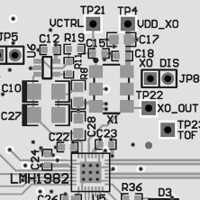
LMH1982 new_layout_image.gif Figure 19. PCB Layout Showing Loop Filter and VCXO