SNLS289D April 2008 – September 2015 LMH1982
PRODUCTION DATA.
- 1 Features
- 2 Applications
- 3 Description
- 4 Revision History
- 5 Pin Configuration and Functions
- 6 Specifications
-
7 Detailed Description
- 7.1 Overview
- 7.2 Functional Block Diagram
- 7.3 Feature Description
- 7.4 Device Functional Modes
- 7.5 Programming
- 7.6
Register Maps
- 7.6.1
I2C Interface Control Register Definitions
- 7.6.1.1 Genlock and Input Reference Control Registers
- 7.6.1.2 Genlock Status And Lock Control Register
- 7.6.1.3 Input Control Register
- 7.6.1.4 PLL 1 Divider Register
- 7.6.1.5 PLL 4 Charge Pump Current Control Register
- 7.6.1.6 Output Clock and TOF Control Register
- 7.6.1.7 TOF Configuration Registers
- 7.6.1.8 PLL 1, 2, 3 Charge Pump Current Control Registers
- 7.6.1.9 Reserved Registers
- 7.6.1
I2C Interface Control Register Definitions
-
8 Application and Implementation
- 8.1
Application Information
- 8.1.1 148.35 MHz PLL Initialization Sequence
- 8.1.2 Enabling Genlock Mode
- 8.1.3 Output Disturbance While Output Alignment Mode Enabled
- 8.1.4 Evaluating the LMH1982
- 8.1.5 Input Reference
- 8.1.6 Output Clocks and TOF
- 8.1.7 Reference And Pll Lock Status
- 8.1.8 Loop Response
- 8.2 Typical Applications
- 8.1
Application Information
- 9 Power Supply Recommendations
- 10Layout
- 11Device and Documentation Support
- 12Mechanical, Packaging, and Orderable Information
8 Application and Implementation
NOTE
Information in the following applications sections is not part of the TI component specification, and TI does not warrant its accuracy or completeness. TI’s customers are responsible for determining suitability of components for their purposes. Customers should validate and test their design implementation to confirm system functionality.
8.1 Application Information
For normal operation, the RESET pin must be set high; otherwise, the device cannot be programmed and will not function properly. To reset the control registers to their default values, toggle RESET low for at least 10 µs and then set high.
The LMH1982 can be configured by programming the control registers via the I2C interface. The I2C slave addresses are DCh for write sequences and DDh for read sequences. The I2C_ENABLE pin must be set low or tied to GND to allow I2C communication; otherwise, the LMH1982 will not acknowledge read/write sequences.
For I2C interface control register map and definitions, refer to I2C Interface Control Register Definitions.
8.1.1 148.35 MHz PLL Initialization Sequence
The following programming sequence is required to initialize PLL 3 and generate a correct 148.35 MHz output once it is selected as the HD_CLK; otherwise, the clock may have duty cycle errors, frequency errors, and/or high jitter. This PLL initialization sequence must be programmed after switching from another HD clock frequency or Hi-Z mode, as well as after a device reset or power cycle condition. Each programming step below represents a separate write sequence.
- Program HD_FREQ = 11b and HD_HIZ = 0 (register 08h) to select 148.35 MHz and enable the HD_CLK output.
- Program a value of 1 to the following register parameters (a single write sequence is valid for this step):
- FB_DIV = 1 (register 04h-05h)
- TOF_RST = 1 (register 09h-0Ah)
- REF_LPFM = 1 (register 0Fh-10h)
- EN_TOF_RST = 1 (register 0Ah)
- Wait at least 2 cycles of the 27 MHz VCXO clock, then program EN_TOF_RST = 0.
After this sequence is completed, the 148.35 MHz clock will operate correctly and normal device configuration can resume. All other output clocks do not require this initialization sequence for proper clock operation.
8.1.2 Enabling Genlock Mode
Upon device power up or reset, the default mode of operation is Free Run mode. To enable Genlock mode, set GNLK = 1 (register 00h). Refer to Genlock Mode for more information.
8.1.3 Output Disturbance While Output Alignment Mode Enabled
When the output alignment mode is enabled (EN_TOF_RST = 1) for a longer period than is required by the output initialization sequence, the output signals can be abruptly phase-aligned to the reference on every output frame. Continual alignment can cause excessive phase “jumps” or jitter on the output clock edge coinciding with the TOF pulse; this effect is unavoidable and can be caused by slight differences in the internal counter reset timing for the TOF generation and also large input jitter. The characteristic of the output jitter can also vary in severity from process variation, part variation, and the selected clock reference frequency. This output jitter can only be inhibited by setting EN_TOF_RST = 0 immediately following the output initialization and before the subsequent output frame.
8.1.4 Evaluating the LMH1982
For information about SDI jitter performance using the LMH1982 with the LMH1981 sync separator, please refer to the following application notes:
- AN-1893: Demonstrating SMPTE-compliant SDI Output Jitter using the LMH1982 and Virtex-5 GTP Transmitter (SNLA110)
- AN-1841: LMH1982 Evaluation Board User Guide (SNVA343)
The LMH1982SQEEVAL Evaluation Board can be ordered from Texas Instrument's website.
8.1.5 Input Reference
The LMH1982 features two reference ports (A and B) with H sync and V sync inputs which are used for phase locking the outputs in Genlock mode. The reference port can be selected by programming RSEL (register 00h). If desired, REF_SEL input can be used instead to select the reference port by initially setting I2C_RSEL = 0 (register 00h).
The reference signals should be 3.3V LVCMOS signals within the input voltage range specified in Electrical Characteristics . The H sync and V sync input signals may have analog timing, such as from the LMH1981 multi-format analog video sync separator, or digital timing, such as from an FPGA SDI deserializer.
8.1.5.1 Reference Frame Decoder
The LMH1982 features an internal frame decoder to determine the reference frame timing from only the H and V sync input timing, which eliminates an extra input pin for an odd/even field timing. The reference frame timing is required to allow for output frame initialization (output TOF and clock alignment) to the reference frame.
To allow for proper frame decoding and subsequent output initialization, the H sync and V sync inputs must comply with the H-V sync timing offset specification, ΔTHV. For interlace formats, the H-V sync timing offset must be within ΔTHV for even fields and be outside ΔTHV for odd fields. Compliance with this specification will ensure the internal frame counters are reset only once per frame. For progressive formats, the H-V timing offset must be within ΔTHV for all frames.
Since the LMH1982 was designed for compatibility with the LMH1981 sync separator, its H and V sync pulses will comply with the ΔTHV specification for any input reference format.
For digital timing from an FPGA SDI deserializer, the recovered H and V sync pulses may be co-timed and be within ΔTHV for both odd and even fields. This will cause the internal frame counters to reset twice per frame and thus preclude proper frame decoding and output initialization. As a simple work-around, the designer may choose to configure the FPGA to gate the V sync signal, allowing only the even field V pulses and gating off the odd field V pulses.
8.1.6 Output Clocks and TOF
The LMH1982 has simultaneous LVDS output SD and HD clocks and an output TOF pulse. For proper output format timing generation and subsequent output initialization, it is highly recommended to follow the programming sequence below:
- Program the output clock frequencies (section Programming the Output Clock Frequencies).
- Program the output format timing (section Output Frame Timing).
- Program the output initialization sequence (section Programming the Output Initialization Sequence).
8.1.6.1 Programming the Output Clock Frequencies
The SD clock frequency can be selected from Table 4 and programmed to SD_FREQ (register 08h). PLL 1 and PLL 4 are used to generate the two SD clock rates but only one SD clock can be selected at a time. If the SD_CLK output is not needed, it can be put in Hi-Z mode by setting SD_HIZ = 1 (register 08h).
If 27 MHz is selected, the VCXO clock is directly converted from a 3.3V single-ended clock at the VCXO input (pin 29) to an LVDS clock at the SD_CLK output port (pins 23 and 24). If 67.5 MHz is selected, the VCXO clock is used as an input reference for PLL 4 to generate this SD clock frequency. In some FPGA SD-SDI SerDes applications, the 67.5 MHz frequency may be required as an SD reference clock instead of the standard 27 MHz frequency.
Table 4. SD Clock Frequency Selection
| SD_CLK (MHz) | SD_FREQ Register 08h |
PLL# |
|---|---|---|
| 27 | 0 | 1 |
| 67.5 | 1 | 4 |
The HD clock frequency can be selected from Table 5 and programmed to HD_FREQ (register 08h). PLL 2 and PLL 3 are used to generate the four different HD clock rates but only one HD clock can be selected at a time. If the HD_CLK output is not needed, it can be put in Hi-Z mode by setting HD_HIZ = 1 (register 08h).
NOTE
If 148.35 MHz is selected, it is required to follow the programming sequence described in 148.35 MHz PLL Initialization Sequence.
Table 5. HD Clock Frequency Selection
| HD_CLK (MHz) | HD_FREQ Register 08h |
PLL# |
|---|---|---|
| 74.25 | 0h | 2 |
| 74.25/1.001 | 1h | 3 |
| 148.5 | 2h | 2 |
| 148.5/1.001 | 3h | 3 |
8.1.6.2 Programming the Output Format Timing
When PLL 1 is stable and locked to the input reference, the output format timing should be specified. The functional block diagram for TOF generation and output initialization is shown in Figure 12.
For proper output generation and initialization, the reference format and output format timings must be fully and correctly programmed to the output format registers 09h–12h, which specify the following:
- Output TOF Clock
- Output Frame Timing
- Reference Frame Timing
- Input-Output Frame Rate Ratio
- Output Frame Line Offset
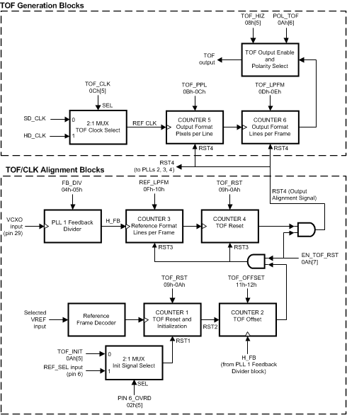 Figure 12. Functional Block Diagram – TOF Generation and Output Initialization Circuitry
8.1.6.2.1 Output TOF Clock
The TOF pulse is derived from a counter chain, which receives either output clock (SD_CLK or HD_CLK) from a 2:1 MUX block, as shown in Figure 12. The TOF clock from the MUX can be selected by programming TOF_CLK (register 0Ch). To select SD_CLK as the TOF clock, set TOF_CLK = 0; otherwise, set TOF_CLK = 1 to select HD_CLK. The selected TOF clock frequency is determined by the SD_FREQ or HD_FREQ register setting.
The TOF output delay time (tD_TOF) for any output format generated from a TOF clock of 27 MHz is specified in Electrical Characteristics. The TOF output delay time for 525i and 1080i/50 generated using 27 MHz and 74.25 MHz, respectively, are shown in Typical Characteristics. The TOF pulse width can be determined by:
where
- fTOF_CLK = Nominal TOF Clock Frequency
- TOF_PPL = Output Format Total Pixels per Line
8.1.6.2.2 Output Frame Timing
The TOF pulse is specified by programming TOF_CLK, TOF_PPL (register 0Bh-0Ch) and TOF_LPFM (register 0Dh-0Eh). These registers configure the 2:1 MUX and output pixel and line counters in the TOF Generation blocks shown in Figure 12. The output frame or TOF pulse rate is determined by:
where
- fTOF_CLK = Nominal TOF Clock Frequency
- TOF_PPL = Output Format Total Pixels per Line
- TOF_LPFM = Output Format Total Lines per Frame
Example:
If the output format is 625i, then:
where
- fTOF_CLK = 27 MHz (SD_FREQ = 0)
- TOF_PPL = 1728
- TOF_LPFM = 625
8.1.6.2.2.1 HD Format TOF Generation Using a 27-MHz TOF Clock
Any HD format TOF pulse can be generated using either: Option 1) its native HD clock frequency, or Option 2) the 27 MHz SD clock frequency.
Using Option 1) for HD output formats can result in TOF output delay being offset by more than one TOF clock period, even after output initialization. This is because the very short period of the HD native clock yields little timing margin for the reset signals to propagate through the internal logic in Figure 12. For example, using a TOF clock of 148.5 MHz gives less than 6.7 ns (< 1 clock cycle) for all the logic to completely synchronize and ensure proper output initialization.
To ensure proper output initialization, Option 2) is recommended for HD output formats, especially 1080p at 50, 59.94, and 60 Hz. This is because the longer period of the 27 MHz clock provides ample timing margin for the internal logic to reset. The output parameters for programming the HD output formats using the 27 MHz clock are shown in Table 2.
To illustrate both TOF clock options, an example is given below for 1080p/59.94, which has a native pixel clock frequency of 148.5/1.001 MHz and frame rate of 60/1.001 Hz:
Option 1) 1080p/59.94 TOF generation using 148.35 MHz
where
- fTOF_CLK = 148.35 MHz (TOF_CLK = 1, HD_FREQ = 3h)
- TOF_PPL = 2200
- TOF_LPFM = 1125
Option 2) 1080p/59.94 TOF generation using 27 MHz
where
- fTOF_CLK = 27 MHz (TOF_CLK = 0, SD_FREQ = 0)
- TOF_PPL = 2002
- TOF_LPFM = 225
As an example, Figure 13 shows a timing illustration for 1080p/59 TOF and clock outputs. Once the outputs are initialized, the SD clock and TOF pulse will have a fixed delay, and the SD clock and HD clock will have a fixed timing offset relative to each other. Therefore, the timing offset between the TOF pulse and HD clock, or tTOF-HD, will also be fixed and can be determined by:
where
- tD_TOF = TOF Output Delay Time referenced to SD_CLK
- tD_SD = SD_CLK Output Delay Time
- tD_HD = HD_CLK Output Delay Time
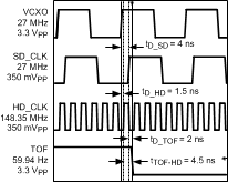 Figure 13. Timing Illustration Showing 1080p/59.94 TOF and CLK Output Delays Using Option 2
8.1.6.2.3 Reference Frame Timing
The reference format frame timing is generated internally and used for resetting the internal counters for output initialization. The reference frame rate should be specified by programming the reference format total lines per frame to REF_LPFM (register 0Fh-10h) as well as the PLL 1 dividers. See Table 2 for programming the parameter values according to each reference format. The reference frame rate is determined by:
where
- fVCXO = 27 MHz Nominal VCXO Clock Frequency
- R_DIV = Reference Divider (not REF_DIV_SEL)
- FB_DIV = Feedback Divider
- REF_LPFM = Reference Format Total Lines per Frame
8.1.6.2.4 Input-Output Frame Rate Ratio
The input-output frame rate ratio is also used for resetting the internal counters for output initialization. The ratio is the Input Frame Rate / Output Frame Rate, in which the numerator and denominator values are reduced to lowest integer factors. The numerator value of this reduced ratio should be programmed to TOF_RST (register 09h-0Ah), and the denominator value is discarded.
Example:
If the input reference is 525i with a frame rate of 30/1.001 Hz and the output format is 625i with a frame rate of 25 Hz, then:
Frame rate ratio = (30/1.001) / 25 = 1200 / 1001
Therefore, the numerator, 1200, should be programmed to TOF_RST.
8.1.6.2.5 Output Frame Line Offset
The output clock and TOF pulse can be aligned to any line of the reference frame by programming TOF_OFFSET (register 11h-12h) and subsequently programming the output initialization sequence. The line offset value should be directly programmed to TOF_OFFSET to delay or advance the outputs' alignment relative to the decoded reference frame timing (see Reference Frame Decoder).
The TOF_OFFSET value must be greater than zero but less than or equal to the programmed value for REF_LPFM (i.e. 0 < TOF_OFFSET ≤ REF_LPFM). If no line offset is required, then program TOF_OFFSET equal to REF_LPFM instead of zero (invalid value).
Example:
If an input reference with PAL timing comes from the LMH1981, the H and V pulses will be aligned to within ΔTHV which occurs on line 313 of the reference. In this case, TOF_OFFSET can be set to 312d (138h) so the output frame will align to Line 1 of the PAL reference (start of frame) after the outputs are initialized. This example is illustrated in Figure 14.
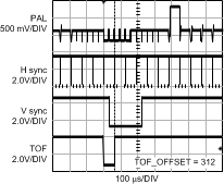 Figure 14. PAL Reference and Output TOF Pulse (TOF_OFFSET = 312)
NOTE
If the alternative set of divider and REF_LPFM values are programmed per (2) for a lower PLL 1 phase comparison frequency, then the output frame cannot be offset to any horizontal line of the reference. Instead, the output frame can only be aligned to the reference in 5 lines steps per 1 step of the TOF_OFFSET value, up to a maximum of reference's total lines per frame divided by 5 (i.e. REF_LPFM). This is because the phase comparison frequency (H_FB signal in Figure 12) will be lower than the H sync input frequency by 5x due to the use of the alternative divider values.
8.1.6.3 Programming the Output Initialization Sequence
Before programming the output initialization (alignment) sequence, the following prerequisites must be met:
- PLL 1 must be stable and locked to the input reference.
- The desired output clock and TOF pulse timing must be fully specified to the output format registers.
To ensure that the output clock and TOF pulse are properly aligned and subsequently phase locked to the reference frame, the output initialization sequence should be programmed accordingly.
During the output frame immediately prior to the frame the initialization is to occur:
- Set EN_TOF_RST = 1(register 0Ah) to enable output alignment mode.
- Toggle TOF_INIT (register 0Ah) from 0 to 1 to reset the internal counters. On the next frame, the output clock and TOF pulse will be initialized (aligned) to the reference frame with line offset programmed to TOF_OFFSET.
- Immediately after the initialization and before the next output frame occurs, clear EN_TOF_RST and TOF_INIT to 0. Otherwise, the output clock will be continually aligned on every output frame while EN_TOF_RST = 1. Continual alignment which may cause excessive jitter on the output clock (from PLL 2, 3, or 4) due to slight differences in the delay paths of the internal logic. This occurrence of excessive clock jitter can be avoided by disabling output alignment mode (EN_TOF_RST = 0) immediately after the initialization sequence.
8.1.6.3.1 TOF Output Delay Considerations
Due to the following conditions, the TOF pulse may be delayed or offset by more than one TOF clock period (tD_TOF > 1 pixel) even after output initialization:
- The delay paths of the internal logic used to generate and align the TOF pulse is greater than one period of the TOF clock. This can occur for HD format TOF pulses generated using the 148 MHz native pixel clock. For HD format TOF generation, it is recommended to use the 27 MHz SD clock as the TOF clock instead of the native HD pixel clock as shown in Output Frame Timing.
- The H sync and/or V sync input pulses have excessive jitter equal to or larger than half of a pixel period of the selected output clock. Input sync jitter less than 3 ns peak-to-peak is recommended.
- PLL 1 is not completely phase locked or stable when the output initialization is performed. The VCXO clock phase error with respect to the H sync input should less than one period of the selected TOF clock.
8.1.6.3.2 Output Clock Initialization Without TOF
For applications that do not require the TOF pulse, it is still necessary to program all output format registers prior to the output initialization sequence. This is because the output initialization circuitry relies on the full and correct specification of the output format. If the TOF output is not needed, it can be put in Hi-Z mode by setting TOF_HIZ = 1 (register 08h).
8.1.6.4 Output Behavior Upon Loss Of Reference
After loss of reference (LOR), the LMH1982 will maintain the TOF pulse without the input reference according to the terminal counts of the reference clock; however, output frequency accuracy will be determined by the VCXO, which may be in Free Run or Holdover operation.
To disable output alignment to an arbitrary reference frame when the reference is reapplied, set EN_TOF_RST = 0 before the reference returns. After PLL 1 has re-locked to the reference, the outputs can be initialized to the desired reference frame.
8.1.7 Reference And Pll Lock Status
The LMH1982 features a reference detector and PLL lock detector that can be used to indicate genlock status of the input reference and device PLLs. Genlock status can be sampled via the NO_REF and NO_LOCK status flag output pins and the REF_VALID, SD_LOCK, and HD_LOCK status bits (register 01h). Both the reference and PLL lock detectors may be programmed for their respective detection thresholds according to the needs of the application system. See Table 7 for a summary of the genlock status bits and status outputs for different conditions.
The NO_REF and NO_LOCK outputs are derived from the genlock status bits and given by the following two logic equations:
NO_REF = REF_VALID
NO_LOCK = (REF_VALID) (SD_LOCK) (HD_LOCK)
8.1.7.1 Reference Detection
In Genlock mode, a valid reference will be indicated by NO_REF = 0 when all the criteria below are met. Otherwise, a loss of reference (LOR) will be indicated by NO_REF = 1.
- An H sync signal is applied to the input reference and conforms to one of the standard formats in Table 2. A V sync signal is not used in reference detection.
- The PLL divide registers are programmed according to the input reference format.
- The control voltage of the VCXO is not within about 500 mV of the GND or VDD supplies.
8.1.7.1.1 Programming the Loss of Reference (LOR) Threshold
The reference detector's error threshold can be programmed to H_ERROR (register 00h), which determines the maximum number of missing H sync pulses before indicating an LOR. The LOR threshold will be the H_ERROR value multiplied by the PLL 1 reference divider value, as shown in Table 6.
Table 6. LOR Threshold Selection
| REF_DIV_SEL Register 03h |
Reference Divider | LOR Threshold |
|---|---|---|
| 0h | 2 | 2 x H_ERROR |
| 1h | 1 | 1 x H_ERROR |
| 2h | 5 | 5 x H_ERROR |
If H_ERROR = 0, then the device will react after the first missing pulse. When the LOR threshold is exceeded, the NO_REF output will indicate LOR, and the device will default to either Free Run or Holdover operation for as long as the reference is lost. As the LOR threshold value is increased, the accuracy for counting the actual number of missing H pulses may diminish due to frequency drifting by PLL 1.
NOTE
If the input reference is missing H pulses periodically, for example every vertical interval period, the PLL may not indicate a valid reference nor achieve lock regardless of the H_ERROR value programmed. This is because periodically missing pulses will translate to a lower average frequency than expected. When the average input frequency falls outside of the absolute pull range (APR) of the VCXO, the PLL will not be able to frequency lock to the input reference.
8.1.7.2 PLL Lock Detection
In Genlock mode, PLL lock will be indicated by NO_LOCK = 0 when all the criteria below are met. Otherwise, a loss of lock will be indicated by NO_LOCK = 1.
- A valid reference is indicated (REF_VALID = 1).
- PLL 1 or PLL 4 is phase locked to the input reference (SD_LOCK = 1).
- PLL 2 or PLL 3 is phase locked to the VCXO clock reference (HD_LOCK = 1).
PLLs 2, 3, and 4 have high loop bandwidths, which allow them to achieve lock quickly and concurrently while PLL 1 achieves lock. Because PLL 1 has a much lower loop bandwidth, it will dictate the overall lock indication time.
8.1.7.2.1 Programming the PLL Lock Threshold
PLL 1's lock detector threshold can be programmed to LOCK_CTRL (register 01h), which determines the maximum phase error between PLL 1's phase detector (PD) inputs before indicating an unlock or lock condition. The PD inputs are the reference signal (H sync input / reference divider) and the feedback signal (VCXO clock / feedback divider).
The lock detector will indicate loss of lock when the phase error between the PD inputs is greater than the lock threshold for three consecutive phase comparison periods. Conversely, it will indicate valid lock when the phase error is less than the lock threshold for three consecutive phase comparison periods.
A larger value for LOCK_CTRL will yield shorter lock indication time (although not actual lock time) at the expense of higher output phase error when lock is initially indicated, whereas a smaller value will yield the opposite effect.
8.1.7.2.2 PLL Lock Status Instability
It is possible for excessive jitter on the H input to indicate lock instability through the NO_LOCK output, even if the VCXO and output clocks are properly phase locked and no system-level errors are occurring (e.g. bit errors). To reduce the probability of false loss of lock indication or lock status instability, LOCK_CTRL can be increased to improve the lock detector’s ability to tolerate a larger amount of input phase jitter or phase error. This can help to ensure the NO_LOCK output and SD_LOCK bit are stable when the reference signal has large input jitter.
Table 7. Summary of Genlock Status Bits and Flag Outputs(1)
| Mode Control Bits Register 00h |
Status Flag Outputs | Status Bits Register 01h |
|||||
|---|---|---|---|---|---|---|---|
| Conditions | GNLK | HOLD-OVER | NO_REF 1
(pin 16) |
NO_LOCK 2
(pin 17) |
HD_LOCK bit 2 |
SD_LOCK bit 1 |
REF_VALID bit 0 |
| Genlock mode,
Reference valid, PLLs locking |
1 | X | 0 | 1 | 0 | 0 | 1 |
| Genlock mode,
Reference valid, PLLs locked |
1 | X | 0 | 0 | 1 | 1 | 1 |
| Genlock mode,
Reference lost, Free Run operation |
1 | 0 | 1 | 1 | 1 | 0 | 0 |
| Genlock mode,
Reference lost, Holdover operation |
1 | 1 | 1 | 1 | 1 | 0 | 0 |
1. NO_REF = REF_VALID
2. NO_LOCK = (REF_VALID) (SD_LOCK) (HD_LOCK)
8.1.8 Loop Response
The overall loop response of the LMH1982 is determined by the design of the VCXO PLL (PLL 1). Because the integrated VCO PLLs use the VCXO clock as the input reference to phase lock the output clocks, the ability of PLL 1 to attenuate the input jitter is critical to output jitter performance, especially low-frequency jitter that occurs at the video line and field rates. The loop response of the LMH1982 can be characterized by PLL 1's loop bandwidth and damping factor.
The loop response is primarily determined by the loop filter components and the loop gain. A passive second-order loop filter consisting of RS, CS, and CP components can provide sufficient input jitter attenuation for most applications, although a higher order passive filter or active filter may also be used. The loop gain is a function of the VCXO gain and programmable PLL parameters.
A lower loop bandwidth will provide higher input jitter attenuation (reduced jitter transfer) for improved output jitter performance; however, increased lock time (or settling time) and larger external component values are a couple trade-offs to a lower loop bandwidth.
8.1.8.1 Loop Response Design Equations
The following equations can be used to design the loop response of PLL 1.
The -3 dB loop bandwidth, BW, can be approximated by:
where
- ICP1 = Nominal VCXO PLL charge pump current (in amps) programmed by setting ICP1 (register 13h).
For example:
ICP1 = 250 µA: ICP1 = 08h (default value)
ICP1 = 0 µA: ICP1 = 00h (min)
ICP1 = 62.5 µA; ICP1 = 02h (practical min)
ICP1 = 968.75 µA; ICP1 = 1Fh (max)
ICP1 step size = 31.25 µA - RS = Nominal value of series resistor (in Ω)
- KVCO = Nominal 27 MHz VCXO gain (in Hz/V)
Nominal 27 MHz VCXO gain (in Hz/V)
KVCO = Pull_range * 27 MHz/Vin_range
For the recommended VCXO (Mftr: CTS, P/N: 357LB3C027M0000): KVCO = 100 ppm * 27 MHz/(3.0V- 0.3V) = 1000 Hz/V - FB_DIV = Feedback Divider value
For example:
FB_DIV =1716 for NTSC timing
Note that this BW approximation does not take into account the effects of the damping factor or the second pole introduced by Cp.
At frequencies far above the −3 dB loop bandwidth, the closed-loop frequency response of PLL 1 will roll off at about −40 dB/decade, which is useful attenuating input jitter at frequencies above the loop bandwidth. Near the −3 dB corner frequency, the roll-off characteristic will depend on other factors, such as damping factor and filter order.
To prevent output jitter due to the modulation of the VCXO by the PLL’s phase comparison frequency:
BW ≤ (27 MHz / FB_DIV) / 20
PLL 1's damping factor, DF, can be approximated by:
where
- CS = Nominal value of the series capacitor (in farads)
A typical design target for DF is between 0.707 to 1, which can often yield a good trade-off between reference spur attenuation and lock time. DF is related to the phase margin, which is a measure of the PLL stability.
A secondary parallel capacitor, CP, is needed to filter the reference spurs introduced by the PLL which may modulate the VCXO input voltage and also cause output jitter. The following relationship should be used to determine CP:
The PLL loop gain, K, can be calculated as:
Therefore, the BW and DF can be expressed in terms of K:
BW = RS * K
DF = (RS/2) * sqrt (CS * K)
8.1.8.1.1 Loop Response Optimization Tips
The need to support various input reference formats will usually require a diverse range of PLL divider values, which can each yield a different loop response assuming all other PLL parameters are kept the same. Typically, it is desired to design and optimize the loop response across all supported input formats without modification to the loop filter circuit. This requires that the loop gain, K, be kept constant across all supported divider values because K affects both BW and DF equations. To keep a narrow range for K, the ratio (ICP1 / feedback divider) should be kept relatively constant. This can be achieved by programming ICP1, so that ICP1 is scaled with FB_DIV for each supported input format.
It is suggested to start designing the loop filter component values from the BW and DF equations with initial assumptions of FB_DIV = 1716 (NTSC) and ICP1 = 250 µA (default setting). Once reasonable component values are achieved under these initial assumptions, it is necessary to check that K can be maintained over the expected range of FB_DIV by adjusting ICP1. The usable current range of ICP1 is limited to a practical minimum of 94 µA (ICP1 = 3d) to a maximum of 969 µA (ICP1 = 31d), which should provide adequate range to maintain a narrow range for K assuming the suggested initial values for FB_DIV and ICP1 were followed. If a narrow range for K cannot be maintained within the usable range of ICP1, then the loop filter design may need to be modified. Some trial-and-error and iterative calculations may be necessary to find an optimal loop filter.
In some loop filter designs, the calculated ICP1 current that is required for a target K value may be near or below the practical minimum of the ICP1 current range. In this scenario, it may also be possible to leverage the programmable reference and feedback dividers by scaling up the values in proportion (i.e. same reduced divider ratio). This would allow ICP1 to be scaled up by the same proportion to be within the usable ICP1 current range and maintain the same K value, since ICP1 and FB_DIV would be scaled by the same factor. For example, by scaling the divider values by a factor of 5x, ICP1 can also be scaled up by 5x such that its within the usable current range. This technique of scaling FB_DIV and ICP1 assumes that the input format has an alternative set of compatible divider values as shown in Table 2.
8.1.8.1.2 Loop Filter Capacitors
It is suggested to use tantalum capacitors for CS and CP instead of ceramic capacitors in the PLL loop filter, which is a sensitive analog circuit. Ferroelectric ceramics, such as X7R, X5R, Y5V, Y5U, etc., exhibit piezoelectric effects that generate electrical noise in response to mechanical vibration and shock. This electrical noise can modulate the VCXO control voltage and consequently induce clock jitter at high amplitudes when the board and ceramic components are subjected to vibration or shock. Tantalum capacitors can be used to mitigate this effect.
8.1.8.2 Lock Time Considerations
The LMH1982 lock time or settling time is determined by the loop response of PLL 1, which has a much lower loop bandwidth compared to the integrated PLLs used to derive the other output clock frequencies. Generally, the lock time is inversely proportional to the loop bandwidth; however, if the loop response is not designed or programmed for sufficient PLL stability, the lock time may not be predicted from the loop bandwidth alone. Therefore, any parameter that affects the loop response can also affect the overall lock time.
One way to reduce lock time is to widen the loop bandwidth by programming a larger or maximum value for ICP1 while PLL 1 is locking; after PLL 1 is locked, ICP1 can be reduced to provide a narrower loop bandwidth while maintaining a reasonable damping factor.
8.1.8.3 VCXO Considerations
The recommended VCXO manufacturer part number is CTS 357LB3C027M0000, which has an absolute pull range (APR) of ±50 ppm and operating temperature range of -20°C to +70°C. A VCXO with a tighter APR can provide better output frequency accuracy in Free Run operation; however, the APR must be wider than the worst-case input frequency error in order to achieve phase lock.
8.1.8.4 Free Run Output Jitter
The input voltage to VC_FREERUN (pin 1) should have sufficient filtering to minimize noise over the frequency bands of interest (i.e. SMPTE SDI jitter frequency bands) which can cause VCXO input voltage modulation and thus free run output clock jitter.
8.2 Typical Applications
8.2.1 Analog Reference Genlock for Triple-Rate SDI Video
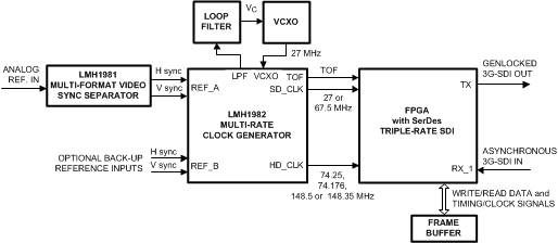 Figure 15. Analog Reference Genlock for Triple-Rate SDI Video
8.2.1.1 Design Requirements
8.2.1.1.1 Programming the PLL 1 Dividers
To genlock the outputs to the reference, it is necessary to phase lock the VCXO clock (PLL 1) to the H sync input signal by programming the PLL dividers. The PLL divider values for each supported input reference format are given in Table 2. The divider values can be determined by reducing the following ratio to its lowest integer factors:
where
- fVCXO = 27 MHz VCXO frequency
- fHSYNC = H sync input frequency
- Feedback Divider = 1 to 8191 (0 is invalid)
- Reference Divider = 1, 2 or 5
Table 8 shows the selection table with compatible PLL 1 reference divider values to program REF_DIV_SEL (register 03h). The PLL 1 feedback divider value can be directly programmed to FB_DIV (register 04h-05h).
Table 8. PLL 1 Reference Divider Selection
| REF_DIV_SEL Register 03h |
Reference Divider |
|---|---|
| 0h | 2 |
| 1h | 1 |
| 2h | 5 |
8.2.1.2 Detailed Design Procedure
8.2.1.2.1 Procedure for Designing the PLL 1 Dividers
Some supported input formats in Table 2 have two sets of compatible divider values: reduced dividers and non-reduced dividers. See Examples 2A and 2B below. Because the loop response of PLL 1 is dependent on the feedback divider value, a lower loop bandwidth and phase comparison frequency can be achieved by programming the non-reduced divider set (see Loop Response).
Examples:
1) For 1080i/59.94 input reference, the dividers are:
- Reference divider = 5 (REF_DIV_SEL = 2h)
- Feedback divider = 4004 (FB_DIV = FA4h)
2A) For 1080i/50 input reference, the reduced dividers are:
- Reference divider = 1 (REF_DIV_SEL = 1h)
- Feedback divider = 960 (FB_DIV = 3C0h)
2B) For 1080i/50 input reference, the non-reduced (alternative) dividers are:
- Reference divider = 5 (REF_DIV_SEL = 2h)
- Feedback divider = 4800 (FB_DIV = 12C0h)
8.2.2 SDI Reference Genlock for Triple-Rate SDI Video
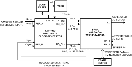 Figure 16. SDI Reference Genlock for Triple-Rate SDI Video
8.2.3 Triple-Rate SDI Loop-through
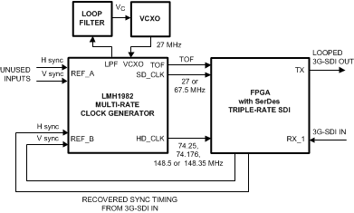 Figure 17. Triple-Rate SDI Loop-through
