ZHCSOW4B September 2021 – March 2022 LM74720-Q1
PRODUCTION DATA
- 1 特性
- 2 应用
- 3 说明
- 4 Revision History
- 5 Pin Configuration and Functions
- 6 Specifications
- 7 Parameter Measurement Information
- 8 Detailed Description
-
9 Application and Implementation
- 9.1 Application Information
- 9.2
Typical 12-V Reverse Battery Protection Application
- 9.2.1 Design Requirements for 12-V Battery Protection
- 9.2.2 Automotive Reverse Battery Protection
- 9.2.3
Detailed Design Procedure
- 9.2.3.1 Design Considerations
- 9.2.3.2 Boost Converter Components (C2, C3, L1)
- 9.2.3.3 Input and Output Capacitance
- 9.2.3.4 Hold-Up Capacitance
- 9.2.3.5 Overvoltage Protection and Battery Monitor
- 9.2.3.6 MOSFET Selection: Blocking MOSFET Q1
- 9.2.3.7 MOSFET Selection: Load Disconnect MOSFET Q2
- 9.2.3.8 TVS Selection
- 9.2.4 Application Curves
- 9.3 Do's and Don'ts
- 10Power Supply Recommendations
- 11Layout
- 12Device and Documentation Support
- 13Mechanical, Packaging, and Orderable Information
9.2.3.5 Overvoltage Protection and Battery Monitor
Resistors R1, R2 and R3 connected in series are used to program the overvoltage threshold and battery monitor ratio. The resistor values required for setting the overvoltage threshold VOV to 37 V and battery monitor ratio VBATT_MON : VBATT to 1:8 are calculated by solving Equation 3 and Equation 4.
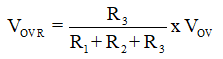
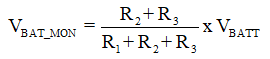
For minimizing the input current drawn from the battery through resistors R1, R2 and R3, TI recommends to use higher value of resistance. Using high value resistors adds error in the calculations because the current through the resistors at higher value become comparable to the leakage current into the OV pin. Maximum leakage current into the OV pin is 1 µA and choosing (R1 + R2 + R3) < 120 kΩ ensures current through resistors is 100 times greater than leakage through OV pin.
Based on the device electrical characteristics, VOVR is 1.23 V and battery monitor ratio (VBATT_MON / VBATT) is designed for a ratio of 1:8. To limit (R1 + R2 + R3) < 120 kΩ, select (R1 + R2) = 100 kΩ. Solving Equation 3 gives R3 = 3.45 kΩ. Solving Equation 4 for R2 using (R1 + R2) = 100 kΩ and R3 = 3.45 kΩ, gives R2 = 9.48 kΩ and R1 = 90.52 kΩ.
Standard 1% resistor values closest to the calculated resistor values are R1 = 90.9 kΩ, R2 = 9.09 kΩ, and R3 = 3.48 kΩ.