ZHCS527G January 2007 – April 2025 LM5574
PRODUCTION DATA
- 1
- 1 特性
- 2 应用
- 3 说明
- 4 Pin Configuration and Functions
- 5 Specifications
- 6 Detailed Description
-
7 Application and Implementation
- 7.1 Application Information
- 7.2
Typical Application
- 7.2.1 Design Requirements
- 7.2.2
Detailed Design Procedure
- 7.2.2.1 Custom Design With WEBENCH® Tools
- 7.2.2.2 External Components
- 7.2.2.3 R3 (R)T
- 7.2.2.4 L1-Inductor
- 7.2.2.5 C3 (C)RAMP
- 7.2.2.6 C9-Output Capacitor
- 7.2.2.7 D1-Async Diode
- 7.2.2.8 C1-Input Capacitor
- 7.2.2.9 C8-VCC Capacitor
- 7.2.2.10 C7-BST Capacitor
- 7.2.2.11 C4- SS Capacitor
- 7.2.2.12 R5, R6- Feedback Resistors
- 7.2.2.13 R1, R2, C2-SD Pin Components
- 7.2.2.14 R4, C5, C6-Compensation Components
- 7.2.2.15 Bias Power Dissipation Reduction
- 7.2.3 Application Curves
- 7.3 Power Supply Recommendations
- 7.4 Layout
- 8 Device and Documentation Support
- 9 Revision History
- 10Mechanical, Packaging, and Orderable Information
6.3.2 Oscillator and Sync Capability
The LM5574 oscillator frequency is set by a single external resistor connected between the RT pin and the AGND pin. The RT resistor must be placed very close to the device and connected directly to the pins of the IC (RT and AGND).To set a desired oscillator frequency (F), the necessary value for the RT resistor can be calculated by Equation 1.

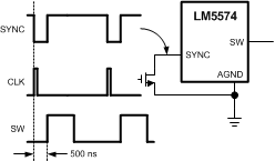
The SYNC pin can be used to synchronize the internal oscillator to an external clock. The external clock must be of higher frequency than the free-running frequency set by the RT resistor. A clock circuit with an open-drain output is the recommended interface from the external clock to the SYNC pin. The clock pulse duration must be greater than 15ns.
 Figure 6-2 Sync From External Clock
 Figure 6-3 Sync From Multiple Devices
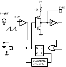
Multiple LM5574 devices can be synchronized together simply by connecting the SYNC pins together. In this configuration, all of the devices are synchronized to the highest frequency device. The diagram in Figure 6-4 shows the SYNC input and output features of the LM5574. The internal oscillator circuit drives the SYNC pin with a strong pulldown and weak pullup inverter. When the SYNC pin is pulled low either by the internal oscillator or an external clock, the ramp cycle of the oscillator is terminated and a new oscillator cycle begins. Thus, if the SYNC pins of several LM5574 ICs are connected together, the IC with the highest internal clock frequency pulls the connected SYNC pins low first and terminate the oscillator ramp cycles of the other ICs. The LM5574 with the highest programmed clock frequency serve as the controller and control the switching frequency of the all the devices with lower oscillator frequency.
 Figure 6-4 Simplified Oscillator Block Diagram and Sync I/O Circuit