ZHCSHU0C March 2018 – October 2021 LM51501-Q1
PRODUCTION DATA
- 1 特性
- 2 应用
- 3 说明
- 4 Revision History
- 5 Device Comparison Table
- 6 Pin Configuration and Functions
- 7 Specifications
-
8 Detailed Description
- 8.1 Overview
- 8.2 Functional Block Diagram
- 8.3
Feature Description
- 8.3.1 Enable (EN Pin)
- 8.3.2 High Voltage VCC Regulator (PVCC, AVCC Pin)
- 8.3.3 Power-On Voltage Selection (VSET Pin)
- 8.3.4 Switching Frequency (RT Pin)
- 8.3.5 Clock Synchronization (SYNC Pin in SS Configuration)
- 8.3.6 Current Sense, Slope Compensation, and PWM (CS Pin)
- 8.3.7 Current Limit (CS Pin)
- 8.3.8 Feedback and Error Amplifier (COMP Pin)
- 8.3.9 Automatic Wake-Up and Standby
- 8.3.10 Boost Status Indicator (STATUS Pin)
- 8.3.11 Maximum Duty Cycle Limit and Minimum Input Supply Voltage
- 8.3.12 MOSFET Driver (LO Pin)
- 8.3.13 Thermal Shutdown
- 8.4 Device Functional Modes
-
9 Application and Implementation
- 9.1 Application Information
- 9.2
Typical Application
- 9.2.1 Design Requirements
- 9.2.2
Detailed Design Procedure
- 9.2.2.1 Custom Design With WEBENCH® Tools
- 9.2.2.2 RSET Resistor
- 9.2.2.3 RT Resistor
- 9.2.2.4 Inductor Selection (LM)
- 9.2.2.5 Current Sense (RS)
- 9.2.2.6 Slope Compensation Ramp (RSL)
- 9.2.2.7 Output Capacitor (COUT)
- 9.2.2.8 Loop Compensation Component Selection and Maximum ESR
- 9.2.2.9 PVCC Capacitor, AVCC Capacitor, and AVCC Resistor
- 9.2.2.10 VOUT Filter (CVOUT, RVOUT)
- 9.2.2.11 Input Capacitor
- 9.2.2.12 MOSFET Selection
- 9.2.2.13 Diode Selection
- 9.2.2.14 Efficiency Estimation
- 9.2.3 Application Curves
- 9.3 System Examples
- 10Power Supply Recommendations
- 11Layout
- 12Device and Documentation Support
- 13Mechanical, Packaging, and Orderable Information
8.4.3.2 Emergency-Call Configuration (EC Configuration)
 Figure 8-8 Typical Emergency Call Application
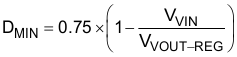
The EC configuration achieves high efficiency at light or medium load by alternating between the wake-up and the low IQ standby modes. In EC configuration, the LM51501-Q1 limits the minimum duty cycle programmed by VVOUT and VVIN. The minimum duty cycle limit is calculated using Equation 12.
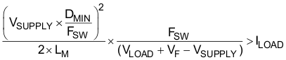
Due to this minimum duty cycle limit, the boost converter sources more current than required when the load current is relatively small. As a result, the output voltage increases and eventually crosses the VOUT standby threshold which is typically 6% higher than the VOUT regulation target. The LM51501-Q1 then goes into the low IQ standby mode. The LM51501-Q1 wakes up when VOUT drops below the VOUT wake-up threshold which is typically 3% higher than the VOUT regulation target. The device alternates between these two modes when the inequality in Equation 13 is true.
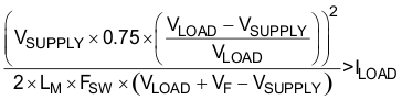
Assuming VLOAD = VVOUT = VVOUT-REG and VSUPPLY = VVIN, the skip cycle operation starts when the inequality in Equation 14 is true.
In EC configuration, the LM51501-Q1 does not generate any pulse if VCOMP is less than the 0.3 V and the required minimum duty cycle limit is zero.
If the peak current limit is triggered before reaching the minimum duty cycle, the device terminates the LO driver output immediately.
If VOUT is greater than the VOUT status-off threshold (typically 12% higher than the VOUT regulation target), the LM51501-Q1 pulls the STATUS pin low.
In EC configuration, light-load efficiency is proportional with the inductor current ripple ratio.
| STATUS | SYNC | RT | COMP | EN | VOUT | PVCC/AVCC | LO | CS | VIN | VSET |
|---|---|---|---|---|---|---|---|---|---|---|
| Released | Enabled in SS configuration | Enabled | Enabled | Enabled | VOUT standby monitor is enabled. VOUT status-off monitor is enabled in EC configuration. | Enabled IPVCC capability ≈ 75 mA | PWM | Enabled | IQ ≈ 30 µA. VIN status-off monitor is enabled in SS configuration | Disabled |
| CONFIGURATION | START-STOP | EMERGENCY-CALL |
|---|---|---|
| VOUT regulation options | 6.0 V, 6.5 V, 9.5 V, 11.5 V | |
| VSET resistor value [Ω] | 29.4k, 19.1k, 9.53k, GND | 90.9k, 71.5k, 54.9k, 41.2k |
| Clock Synchronization | Yes | No, SYNC should be grounded |
| VOUT wake-up threshold [V] | VVOUT-REG × 1.03 | |
| VOUT standby threshold [V] | VVOUT-REG × 1.24 | VVOUT-REG × 1.06 |
| VOUT status-off threshold [V] | N/A | VVOUT-REG × 1.12 |
| VIN standby threshold [V] | VVOUT-REG × 1.03 + 1.0 V | N/A |
| STATUS pin control (Open-drain with pullup resistor) | Released by VOUT wake-up Pulled down by VIN standby | Released by VOUT wake-up Pulled down by VOUT status-off |
| At heavy load when VVIN « VVOUT | Pulse width modulation (PWM) | |
| At light or no load when VVIN « VVOUT | LO turns on at every cycle in wake-up configuration. Skip cycle operation by alternating between wake-up and standby configurations. | |
| Minimum on-time is limited | Minimum duty cycle is limited | |
| When VVIN ≈ VVOUT or VVIN ≥ VVOUT | LO turns on at every cycle in wake-up configuration. On-time is limited by TON-MIN. VOUT goes out of regulation. | Duty cycle can drop to 0%. No pulses if VCOMP < 0.3 V and DMIN ≤ 0%. |
| Maximum duty-cycle limit | Typically 87% | |