ZHCSHU0C March 2018 – October 2021 LM51501-Q1
PRODUCTION DATA
- 1 特性
- 2 应用
- 3 说明
- 4 Revision History
- 5 Device Comparison Table
- 6 Pin Configuration and Functions
- 7 Specifications
-
8 Detailed Description
- 8.1 Overview
- 8.2 Functional Block Diagram
- 8.3
Feature Description
- 8.3.1 Enable (EN Pin)
- 8.3.2 High Voltage VCC Regulator (PVCC, AVCC Pin)
- 8.3.3 Power-On Voltage Selection (VSET Pin)
- 8.3.4 Switching Frequency (RT Pin)
- 8.3.5 Clock Synchronization (SYNC Pin in SS Configuration)
- 8.3.6 Current Sense, Slope Compensation, and PWM (CS Pin)
- 8.3.7 Current Limit (CS Pin)
- 8.3.8 Feedback and Error Amplifier (COMP Pin)
- 8.3.9 Automatic Wake-Up and Standby
- 8.3.10 Boost Status Indicator (STATUS Pin)
- 8.3.11 Maximum Duty Cycle Limit and Minimum Input Supply Voltage
- 8.3.12 MOSFET Driver (LO Pin)
- 8.3.13 Thermal Shutdown
- 8.4 Device Functional Modes
-
9 Application and Implementation
- 9.1 Application Information
- 9.2
Typical Application
- 9.2.1 Design Requirements
- 9.2.2
Detailed Design Procedure
- 9.2.2.1 Custom Design With WEBENCH® Tools
- 9.2.2.2 RSET Resistor
- 9.2.2.3 RT Resistor
- 9.2.2.4 Inductor Selection (LM)
- 9.2.2.5 Current Sense (RS)
- 9.2.2.6 Slope Compensation Ramp (RSL)
- 9.2.2.7 Output Capacitor (COUT)
- 9.2.2.8 Loop Compensation Component Selection and Maximum ESR
- 9.2.2.9 PVCC Capacitor, AVCC Capacitor, and AVCC Resistor
- 9.2.2.10 VOUT Filter (CVOUT, RVOUT)
- 9.2.2.11 Input Capacitor
- 9.2.2.12 MOSFET Selection
- 9.2.2.13 Diode Selection
- 9.2.2.14 Efficiency Estimation
- 9.2.3 Application Curves
- 9.3 System Examples
- 10Power Supply Recommendations
- 11Layout
- 12Device and Documentation Support
- 13Mechanical, Packaging, and Orderable Information
9.2.2.7 Output Capacitor (COUT)
There are a few ways to select the proper value of output capacitor (COUT). The output capacitor value can be selected based on output voltage ripple, output overshoot, or output undershoot due to load transient. In this example, COUT is selected based on output undershoot because the wake-up performance is similar with no-load to full-load transient performance.
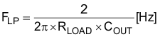
The output undershoot becomes smaller by increasing FCROSS or by decreasing FLP. A smaller COUT is allowed by increasing FCROSS or by decreasing FLP.
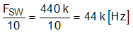
To increase FCROSS, FSW and FRHP must be increased because the maximum FCROSS is, in general, limited at 1/10 of FRHP at VSUPPLY(MIN) or 1/10 of FSW, whichever is lower.
FRHP is calculated using Equation 28.
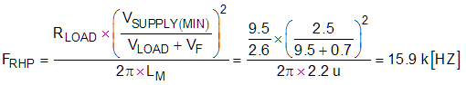
FCROSS is selected at 1/10 of FRHP or 1/10 of FSW, whichever is lower.
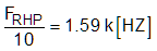
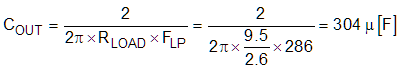
In this example, 1.59 kHz is selected as a target FCROSS and FLP is selected to be 286 Hz (K1 = 0.18).
In general, there is about 5% or less undershoot with FLP = 0.1 × FCROSS (K1 = 0.1) and 10% or less undershoot with FLP = 0.2 × FCROSS (K1 = 0.2) during 0% to 100% load transient. The recommended K1 factor range is from 0.02 to 0.2.
FLP is calculated using Equation 31.
The minimum required output capacitance value is calculated using Equation 32.
The maximum output ripple current is calculated at the minimum input supply voltage using Equation 33:
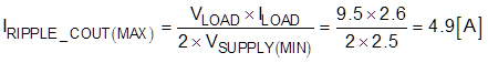
The ripple current rating of the output capacitors must be enough to handle the output ripple current. By using multiple output capacitors, the ripple current can be split. In practice, ceramic capacitors are placed closer to the diode and the MOSFET than the bulk aluminum capacitors to absorb the majority of the ripple current.
In this example, three 100-µF capacitors are placed in parallel to ensure ripple current capability. If high-ESR capacitors are used for the output capacitor, additional 10-µF ceramic capacitors can be placed close to the switching components to minimize switching noise.