ZHCSHU0C March 2018 – October 2021 LM51501-Q1
PRODUCTION DATA
- 1 特性
- 2 应用
- 3 说明
- 4 Revision History
- 5 Device Comparison Table
- 6 Pin Configuration and Functions
- 7 Specifications
-
8 Detailed Description
- 8.1 Overview
- 8.2 Functional Block Diagram
- 8.3
Feature Description
- 8.3.1 Enable (EN Pin)
- 8.3.2 High Voltage VCC Regulator (PVCC, AVCC Pin)
- 8.3.3 Power-On Voltage Selection (VSET Pin)
- 8.3.4 Switching Frequency (RT Pin)
- 8.3.5 Clock Synchronization (SYNC Pin in SS Configuration)
- 8.3.6 Current Sense, Slope Compensation, and PWM (CS Pin)
- 8.3.7 Current Limit (CS Pin)
- 8.3.8 Feedback and Error Amplifier (COMP Pin)
- 8.3.9 Automatic Wake-Up and Standby
- 8.3.10 Boost Status Indicator (STATUS Pin)
- 8.3.11 Maximum Duty Cycle Limit and Minimum Input Supply Voltage
- 8.3.12 MOSFET Driver (LO Pin)
- 8.3.13 Thermal Shutdown
- 8.4 Device Functional Modes
-
9 Application and Implementation
- 9.1 Application Information
- 9.2
Typical Application
- 9.2.1 Design Requirements
- 9.2.2
Detailed Design Procedure
- 9.2.2.1 Custom Design With WEBENCH® Tools
- 9.2.2.2 RSET Resistor
- 9.2.2.3 RT Resistor
- 9.2.2.4 Inductor Selection (LM)
- 9.2.2.5 Current Sense (RS)
- 9.2.2.6 Slope Compensation Ramp (RSL)
- 9.2.2.7 Output Capacitor (COUT)
- 9.2.2.8 Loop Compensation Component Selection and Maximum ESR
- 9.2.2.9 PVCC Capacitor, AVCC Capacitor, and AVCC Resistor
- 9.2.2.10 VOUT Filter (CVOUT, RVOUT)
- 9.2.2.11 Input Capacitor
- 9.2.2.12 MOSFET Selection
- 9.2.2.13 Diode Selection
- 9.2.2.14 Efficiency Estimation
- 9.2.3 Application Curves
- 9.3 System Examples
- 10Power Supply Recommendations
- 11Layout
- 12Device and Documentation Support
- 13Mechanical, Packaging, and Orderable Information
9.2.2.8 Loop Compensation Component Selection and Maximum ESR
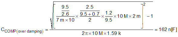
Based on Equation 18, CCOMP is calculated using Equation 34 and Equation 35:
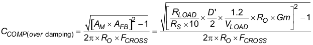
By selecting CCOMP following Equation 34, the typical phase margin is set to 90⁰ and the loop response is overdamped. In this example, FZ_EA is placed at a frequency 3 times higher than the FLP to have lower phase margin but faster settling time (K2 = 3, target FZ_EA is 860 Hz). The recommended range of FZ_EA is from 1 × FLP to 4 × FLP (1 ≤ K2 ≤ 4). Practical crossover frequency will vary with K2 with a range of 0.5 × FCROSS to 1.0 × FCROSS.
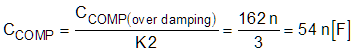
A standard value of 56 nF is chosen for CCOMP.
RCOMP is selected to set the error amplifier zero at 860 Hz.
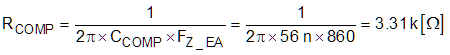
A standard value of 3.32 kΩ is chosen for RCOMP.
CHF is usually used to create a pole at high frequency (FP_EA) to cancel FZ_ESR. By using a small ESR capacitor that can place FZ_ESR greater than 10 × FCROSS, the output capacitor ESR would not affect the loop stability. The maximum ESR which does not affect the loop response is calculated using Equation 38.
