ZHCSJC9G September   2006  – Jaunuary 2020 LM5069

PRODUCTION DATA.  

  1. 特性
  2. 应用
  3. 说明
    1.     Device Images
      1.      典型应用图
  4. 修订历史记录
    1.     Device Comparison
  5. Pin Configuration and Functions
    1.     Pin Functions
  6. Specifications
    1. 6.1 Absolute Maximum Ratings
    2. 6.2 ESD Ratings
    3. 6.3 Recommended Operating Conditions
    4. 6.4 Thermal Information
    5. 6.5 Electrical Characteristics
    6. 6.6 Typical Characteristics
  7. Detailed Description
    1. 7.1 Overview
    2. 7.2 Functional Block Diagram
    3. 7.3 Feature Description
      1. 7.3.1 Current Limit
      2. 7.3.2 Circuit Breaker
      3. 7.3.3 Power Limit
      4. 7.3.4 Undervoltage Lockout (UVLO)
      5. 7.3.5 Overvoltage Lockout (OVLO)
      6. 7.3.6 Power Good Pin
    4. 7.4 Device Functional Modes
      1. 7.4.1 Power Up Sequence
      2. 7.4.2 Gate Control
      3. 7.4.3 Fault Timer and Restart
      4. 7.4.4 Shutdown Control
  8. Application and Implementation
    1. 8.1 Application Information
    2. 8.2 Typical Application
      1. 8.2.1 48-V, 10-A Hot Swap Design
        1. 8.2.1.1 Design Requirements
        2. 8.2.1.2 Detailed Design Procedure
          1. 8.2.1.2.1 Select RSNS and CL setting
          2. 8.2.1.2.2 Selecting the Hot Swap FET(s)
          3. 8.2.1.2.3 Select Power Limit
          4. 8.2.1.2.4 Set Fault Timer
          5. 8.2.1.2.5 Check MOSFET SOA
          6. 8.2.1.2.6 Set Undervoltage and Overvoltage Threshold
            1. 8.2.1.2.6.1 Option A
            2. 8.2.1.2.6.2 Option B
            3. 8.2.1.2.6.3 Option C
            4. 8.2.1.2.6.4 Option D
          7. 8.2.1.2.7 Input and Output Protection
          8. 8.2.1.2.8 Final Schematic and Component Values
        3. 8.2.1.3 Application Curves
  9. Power Supply Recommendations
  10. 10Layout
    1. 10.1 Layout Guidelines
      1. 10.1.1 PC Board Guidelines
      2. 10.1.2 System Considerations
    2. 10.2 Layout Example
  11. 11器件和文档支持
    1. 11.1 器件支持
      1. 11.1.1 开发支持
    2. 11.2 文档支持
      1. 11.2.1 相关文档
    3. 11.3 接收文档更新通知
    4. 11.4 社区资源
    5. 11.5 商标
    6. 11.6 静电放电警告
    7. 11.7 Glossary
  12. 12机械、封装和可订购信息

封装选项

机械数据 (封装 | 引脚)
散热焊盘机械数据 (封装 | 引脚)
订购信息

Option B

If all four thresholds must be accurately defined, the configuration in Figure 31 can be used.
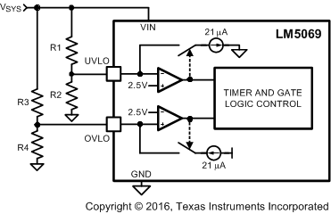
LM5069 20197241.gifFigure 31. Programming the Four Thresholds

The four resistor values are calculated as follows:

  1. Choose the upper UVLO threshold (VUVH) and lower UVLO threshold (VUVL) with Equation 34 and Equation 35.
  2. Equation 34. LM5069 20197230.gif
    Equation 35. LM5069 20197243.gif
  3. Choose the upper OVLO threshold (VOVH) and lower OVLO threshold (VOVL) with Equation 36 and Equation 37.
  4. Equation 36. LM5069 20197244.gif
    Equation 37. LM5069 20197245.gif

As an example, assume the application requires the following thresholds: VUVH = 22 V, VUVL = 17 V, VOVH = 60 V, and VOVL = 58 V. Therefore VUV(HYS) = 5 V, and VOV(HYS) = 2 V. The resistor values are:

  • R1 = 238 kΩ, R2 = 41 kΩ
  • R3 = 95.2 kΩ, R4 = 4.14 kΩ

Where the R1-R4 resistor values are known, the threshold voltages and hysteresis are calculated from Equation 38 to Equation 43.

Equation 38. LM5069 20197246.gif
Equation 39. LM5069 20197247.gif
Equation 40. VUV(HYS) = R1 x 21 µA
Equation 41. LM5069 20197248.gif
Equation 42. LM5069 20197249.gif
Equation 43. VOV(HYS) = R3 x 21 µA