ZHCSCT1A April 2014 – August 2014 LM5066I
PRODUCTION DATA.
- 1 特性
- 2 应用
- 3 说明
- 4 简化电路原理图
- 5 修订历史记录
- 6 Device Comparison Table
- 7 Pin Configuration and Functions
- 8 Specifications
-
9 Detailed Description
- 9.1 Overview
- 9.2 Functional Block Diagram
- 9.3 Feature Description
- 9.4 Device Functional Modes
- 9.5
Programming
- 9.5.1 PMBus Command Support
- 9.5.2
Standard PMBus Commands
- 9.5.2.1 OPERATION (01h)
- 9.5.2.2 CLEAR_FAULTS (03h)
- 9.5.2.3 CAPABILITY (19h)
- 9.5.2.4 VOUT_UV_WARN_LIMIT (43h)
- 9.5.2.5 OT_FAULT_LIMIT (4Fh)
- 9.5.2.6 OT_WARN_LIMIT (51h)
- 9.5.2.7 VIN_OV_WARN_LIMIT (57h)
- 9.5.2.8 VIN_UV_WARN_LIMIT (58h)
- 9.5.2.9 STATUS_BYTE (78h)
- 9.5.2.10 STATUS_WORD (79h)
- 9.5.2.11 STATUS_VOUT (7Ah)
- 9.5.2.12 STATUS_INPUT (7Ch)
- 9.5.2.13 STATUS_TEMPERATURE (7dh)
- 9.5.2.14 STATUS_CML (7Eh)
- 9.5.2.15 STATUS_OTHER (7Fh)
- 9.5.2.16 STATUS_MFR_SPECIFIC (80h)
- 9.5.2.17 READ_EIN (86h)
- 9.5.2.18 READ_VIN (88h)
- 9.5.2.19 READ_IIN (89h)
- 9.5.2.20 READ_VOUT (8Bh)
- 9.5.2.21 READ_TEMPERATURE_1 (8Dh)
- 9.5.2.22 READ_PIN (97h)
- 9.5.2.23 MFR_ID (99h)
- 9.5.2.24 MFR_MODEL (9Ah)
- 9.5.2.25 MFR_REVISION (9Bh)
- 9.5.3
Manufacturer Specific PMBus Commands
- 9.5.3.1 MFR_SPECIFIC_00: READ_VAUX (D0h)
- 9.5.3.2 MFR_SPECIFIC_01: MFR_READ_IIN (D1h)
- 9.5.3.3 MFR_SPECIFIC_02: MFR_READ_PIN (D2h)
- 9.5.3.4 MFR_SPECIFIC_03: MFR_IN_OC_WARN_LIMIT (D3h)
- 9.5.3.5 MFR_SPECIFIC_04: MFR_PIN_OP_WARN_LIMIT (D4h)
- 9.5.3.6 MFR_SPECIFIC_05: READ_PIN_PEAK (D5h)
- 9.5.3.7 MFR_SPECIFIC_06: CLEAR_PIN_PEAK (D6h)
- 9.5.3.8 MFR_SPECIFIC_07: GATE_MASK (D7h)
- 9.5.3.9 MFR_SPECIFIC_08: ALERT_MASK (D8h)
- 9.5.3.10 MFR_SPECIFIC_09: DEVICE_SETUP (D9h)
- 9.5.3.11 MFR_SPECIFIC_10: BLOCK_READ (DAh)
- 9.5.3.12 MFR_SPECIFIC_11: SAMPLES_FOR_AVG (DBh)
- 9.5.3.13 MFR_SPECIFIC_12: READ_AVG_VIN (DCh)
- 9.5.3.14 MFR_SPECIFIC_13: READ_AVG_VOUT (DDh)
- 9.5.3.15 MFR_SPECIFIC_14: READ_AVG_IIN (DEh)
- 9.5.3.16 MFR_SPECIFIC_14: READ_AVG_PIN (DFh)
- 9.5.3.17 MFR_SPECIFIC_15: READ_AVG_PIN
- 9.5.3.18 MFR_SPECIFIC_16: BLACK_BOX_READ (E0h)
- 9.5.3.19 MFR_SPECIFIC_17: READ_DIAGNOSTIC_WORD (E1h)
- 9.5.3.20 MFR_SPECIFIC_18: AVG_BLOCK_READ (E2h)
- 9.5.4 Reading and Writing Telemetry Data and Warning Thresholds
- 9.5.5 Determining Telemetry Coefficients Empirically With Linear Fit
- 9.5.6 Writing Telemetry Data
- 9.5.7 PMBus Address Lines (ADR0, ADR1, ADR2)
- 9.5.8 SMBA Response
-
10Application and Implementation
- 10.1 Application Information
- 10.2
Typical Application
- 10.2.1
48-V, 10-A PMBus Hotswap Design
- 10.2.1.1 Design Requirements
- 10.2.1.2
Detailed Design-In Procedure
- 10.2.1.2.1 Select RSNS and CL Setting
- 10.2.1.2.2 Selecting the Hotswap FETs
- 10.2.1.2.3 Select Power Limit
- 10.2.1.2.4 Set Fault Timer
- 10.2.1.2.5 Check MOSFET SOA
- 10.2.1.2.6 Set UVLO and OVLO Thresholds
- 10.2.1.2.7 Power Good Pin
- 10.2.1.2.8 Input and Output Protection
- 10.2.1.2.9 Final Schematic and Component Values
- 10.2.1.3 Application Curves
- 10.2.2
48-V, 20-A PMBus Hotswap Design
- 10.2.2.1 Design Requirements
- 10.2.2.2
Detailed Design Procedure
- 10.2.2.2.1 Selecting the Sense Resistor and CL Setting
- 10.2.2.2.2 Selecting the Hotswap FETs
- 10.2.2.2.3 Select Power Limit
- 10.2.2.2.4 Set Fault Timer
- 10.2.2.2.5 Check MOSFET SOA
- 10.2.2.2.6 Switching to dv/dt-Based Start-Up
- 10.2.2.2.7 Choosing the VOUT Slew Rate
- 10.2.2.2.8 Select Power Limit and Fault Timer
- 10.2.2.2.9 Chose Input and Output Protection and Set Undervoltage, Overvoltage, and Power Good Thresholds
- 10.2.2.2.10 Final Schematic and Component Values
- 10.2.2.3 Application Curves
- 10.2.1
48-V, 10-A PMBus Hotswap Design
- 11Power Supply Recommendations
- 12Layout
- 13器件和文档支持
- 14机械封装和可订购信息
8 Specifications
8.1 Handling Ratings
| MIN | MAX | UNIT | |||
|---|---|---|---|---|---|
| Tstg | Storage temperature | –65 | 150 | °C | |
| VESD(1) | Electrostatic discharge | Human body model (HBM), per ANSI/ESDA/JEDEC JS-001, all pins except GATE(2) | –2 | 2 | kV |
| Charged device model (CDM), per JEDEC specification JESD22-C101, all pins(3) | –500 | 500 | V | ||
(1) The human body model is a 100-pF capacitor discharged through a 1.5-kΩ resistor into each pin. 2-kV rating for all pins except GATE which is rated for 1 kV.
(2) JEDEC document JEP155 states that 500-V HBM allows safe manufacturing with a standard ESD control process.
(3) JEDEC document JEP157 states that 250-V CDM allows safe manufacturing with a standard ESD control process.
8.2 Recommended Operating Conditions
over operating free-air temperature range (unless otherwise noted)| MIN | NOM | MAX | UNIT | ||
|---|---|---|---|---|---|
| VIN, SENSE, OUT voltage | 10 | 80 | V | ||
| Junction temperature | –40 | 125 | °C | ||
8.3 Thermal Information
| THERMAL METRIC(1) | LM5066I | UNIT | |
|---|---|---|---|
| PWP | |||
| 28 PINS | |||
| RθJA | Junction-to-ambient thermal resistance(2) | 35.6 | °C/W |
| RθJC(top) | Junction-to-case (top) thermal resistance(3) | 19.9 | |
| RθJB | Junction-to-board thermal resistance(4) | 16.8 | |
| ψJT | Junction-to-top characterization parameter(5) | 0.5 | |
| ψJB | Junction-to-board characterization parameter(6) | 16.7 | |
| RθJC(bot) | Junction-to-case (bottom) thermal resistance(7) | 2.9 | |
(1) For more information about traditional and new thermal metrics, see the IC Package Thermal Metrics application report, SPRA953.
(2) The junction-to-ambient thermal resistance under natural convection is obtained in a simulation on a JEDEC-standard, high-K board, as specified in JESD51-7, in an environment described in JESD51-2a.
(3) The junction-to-case (top) thermal resistance is obtained by simulating a cold plate test on the package top. No specific JEDEC-standard test exists, but a close description can be found in the ANSI SEMI standard G30-88.
(4) The junction-to-board thermal resistance is obtained by simulating in an environment with a ring cold plate fixture to control the PCB temperature, as described in JESD51-8.
(5) The junction-to-top characterization parameter, ψJT, estimates the junction temperature of a device in a real system and is extracted from the simulation data for obtaining θJA, using a procedure described in JESD51-2a (sections 6 and 7).
(6) The junction-to-board characterization parameter, ψJB, estimates the junction temperature of a device in a real system and is extracted from the simulation data for obtaining θJA , using a procedure described in JESD51-2a (sections 6 and 7).
(7) The junction-to-case (bottom) thermal resistance is obtained by simulating a cold plate test on the exposed (power) pad. No specific JEDEC standard test exists, but a close description can be found in the ANSI SEMI standard G30-88.
8.4 Electrical Characteristics
Unless otherwise stated, the following conditions apply: VVIN = 48 V, –40°C < TJ < 125°C, VUVLO = 3 V , VOVLO = 0 V, RPWR= 20 kΩ. See (1).| PARAMETER | TEST CONDITIONS | MIN | TYP | MAX | UNIT | |
|---|---|---|---|---|---|---|
| INPUT (VIN PIN) | ||||||
| IIN-EN | Input current, enabled | VUVLO = 3 V and VOVLO = 2 V | 5.6 | 7 | mA | |
| PORIT | Power-on reset threshold at VVIN to trigger insertion timer | VVIN increasing | 7.8 | 9.0 | V | |
| POREN | Power-on reset threshold at VVIN to enable all functions | VVIN increasing | 8.6 | 9.9 | V | |
| PORHYS | POREN hysteresis | VVIN decreasing | 100 | mV | ||
| VDD REGULATOR (VDD PIN) | ||||||
| VDD | IVDD = 0 mA | 4.60 | 4.90 | 5.15 | V | |
| IVDD = 10 mA | 4.60 | 4.85 | 5.15 | V | ||
| VDDILIM | VVDD current limit | –50 | –30 | –15 | mA | |
| VDDPOR | VVDD voltage reset threshold | VVDD rising | 4.1 | V | ||
| UVLO/EN, OVLO PINS | ||||||
| UVLOTH | UVLO threshold | VUVLO falling | 2.41 | 2.48 | 2.55 | V |
| UVLOHYS | UVLO hysteresis current | VUVLO = 1 V | 16 | 20 | 24 | µA |
| UVLOBIAS | UVLO bias current | VUVLO = 3 V | 1 | µA | ||
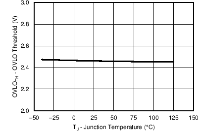
| OVLOTH | OVLO threshold | VOVLO rising | 2.39 | 2.46 | 2.53 | V |
| OVLOHYS | OVLO hysteresis current | VOVLO= 1 V | –24 | –21 | –16 | µA |
| OVLOBIAS | OVLO bias current | VOVLO = 1 V | 1 | µA | ||
| POWER GOOD (PGD PIN) | ||||||
| PGDVOL | Output low voltage | ISINK = 2 mA | 100 | 400 | mV | |
| PGDIOH | Off leakage current | VPGD = 80 V | 1 | µA | ||
| FB PIN | ||||||
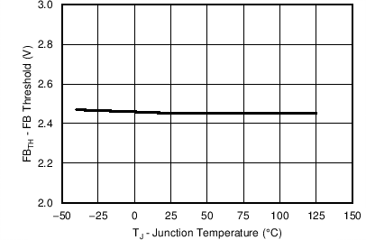
| FBTH | FB threshold | VUVLO = 3 V and VOVLO = 2 V | 2.41 | 2.46 | 2.52 | V |
| FBHYS | FB hysteresis current | –25 | –20 | –15 | µA | |
| FBLEAK | Off leakage current | VFB = 2.3 V | 1 | µA | ||
| POWER LIMIT (PWR PIN) | ||||||
| Power limit sense voltage (VVIN_K – VSENSE) | VSENSE – VOUT = 48 V, RPWR = 60 kΩ | 7.4 | 9.4 | 11.4 | mV | |
| VSENSE – VOUT = 48 V, RPWR = 20 kΩ | 1.5 | 3.5 | 5.7 | mV | ||
| VSENSE – VOUT = 48 V, RPWR = 20 kΩ, TJ = 0°C to 85°C |
1.85 | 3.5 | 5.02 | mV | ||
| VSENSE – VOUT = 24 V, RPWR = 60 kΩ | 15 | 18.75 | 22.5 | mV | ||
| VSENSE – VOUT = 24 V, RPWR = 20 kΩ | 5 | 7.23 | 10 | mV | ||
| IPWR | PWR pin current | VPWR = 2.5 V | -20 | µA | ||
| RSAT(PWR) | PWR pin impedance when disabled | VUVLO = 2 V | 120 | Ω | ||
| GATE CONTROL (GATE PIN) | ||||||
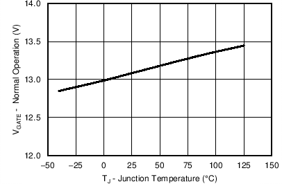
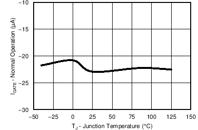
| IGATE | Source current | Normal operation | –40 | –20 | –7.5 | µA |
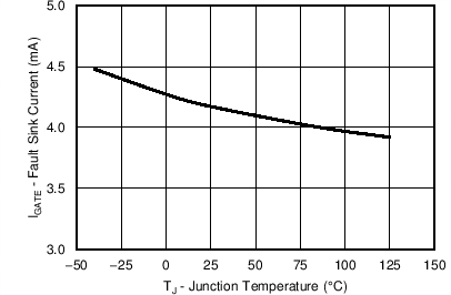
| Fault sink current | VUVLO = 2 V | 3.4 | 4.2 | 5.3 | mA | |
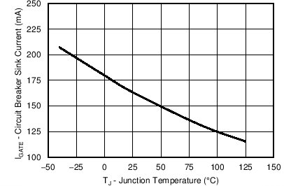
| POR circuit breaker sink current | VVIN_K – VSENSE = 60 mV or VVIN < PORIT, VGATE = 5 V, OUT = 0 V, CB/CL ratio bit = 0, CL = 1 |
90 | 160 | 230 | mA | |
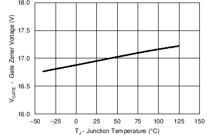
| VGATEZ | Reverse-bias voltage of GATE to OUT Zener diode, IZ = –100 µA | VGATE– VOUT | 15 | 16.5 | 18 | V |
| VGATECP | Peak charge pump voltage in normal operation (VIN = VOUT) |
VGATE– VOUT | 11 | 13 | 15 | V |
| OUT PIN | ||||||
| IOUT-EN | OUT bias current, enabled | VIN = VOUT, normal operation | 60 | 80 | 100 | µA |
| IOUT-DIS | OUT bias current, disabled (2) | Disabled, OUT = 0 V, VVIN_K = VSENSE | –65 | –50 | –35 | µA |
| CURRENT LIMIT | ||||||
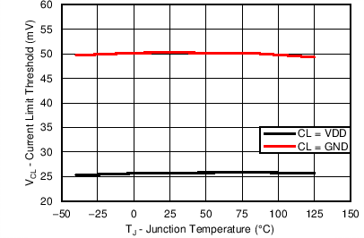
| VCL | Current limit threshold voltage (VVIN_K – VSENSE) |
CL = VDD | 23.4 | 26 | 28.6 | mV |
| CL = GND | 45 | 50 | 55 | |||
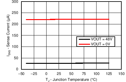
| ISENSE | SENSE input current | Enabled, SENSE = OUT | 20 | 25 | 35 | µA |
| Disabled, OUT = 0 V | 66 | |||||
| Enabled, OUT = 0 V | 190 | 220 | 250 | |||
| CIRCUIT BREAKER | ||||||
| RTCB | Circuit breaker to current limit ratio: (VVIN_K – VSENSE)CB/VCL |
CB/CL ratio bit = 0, ILIM = 50 mV | 1.64 | 1.94 | 2.23 | V/V |
| CB/CL ratio bit = 1, ILIM = 50 mV | 3.28 | 3.87 | 4.45 | |||
| CB/CL ratio bit = 0, ILIM = 26 mV | 1.5 | 1.88 | 2.3 | |||
| CB/CL ratio bit = 1, ILIM = 26 mV | 3.1 | 3.75 | 4.45 | |||
| VCB | Circuit breaker threshold voltage: (VVIN_K – VSENSE) | CB/CL ratio bit = 0, ILIM = 50 mV | 76 | 96 | 116 | mV |
| CB/CL ratio bit = 1, ILIM = 50 mV | 155 | 193 | 235 | |||
| CB/CL ratio bit = 0, ILIM = 26 mV | 38 | 48 | 58 | |||
| CB/CL ratio bit = 1, ILIM = 26 mV | 76 | 96 | 116 | |||
| TIMER (TIMER PIN) | ||||||
| VTMRH | Upper threshold | 3.74 | 3.9 | 4.07 | V | |
| VTMRL | Lower threshold | Restart cycles | 1 | 1.2 | 1.4 | V |
| End of eighth cycle re-enable threshold | 0.3 | V | ||||
| ITIMER | Insertion time current | TIMER pin = 2 V | –5.9 | –4.8 | –3.3 | µA |
| Sink current, end of insertion time | 0.9 | 1.5 | 2.1 | mA | ||
| Fault detection current | –90 | –75 | –60 | µA | ||
| Fault sink current | 1.7 | 2.5 | 3.2 | µA | ||
| DCFAULT | Fault restart duty cycle | 0.5% | ||||
| INTERNAL REFERENCE | ||||||
| VREF | Reference voltage | 2.93 | 2.97 | 3.02 | V | |
| ADC AND MUX | ||||||
| Resolution | 12 | Bits | ||||
| INL | Integral non-linearity | ADC only | ±4 | LSB | ||
| tACQUIRE | Acquisition + conversion time | Any channel | 100 | µs | ||
| tRR | Acquisition round robin time | Cycle all channels | 1 | ms | ||
| TELEMETRY ACCURACY | ||||||
| IINFSR | Current input full-scale range | CL = GND | 50 | 54.4 | 58 | mV |
| CL = VDD | 26 | 27.0 | 29 | mV | ||
| IINLSB | Current input LSB | CL = GND | 13.30 | µV | ||
| CL = VDD | 6.70 | µV | ||||
| VAUXFSR | VAUX input full-scale range | 2.93 | 2.97 | 3.01 | V | |
| VAUXLSB | VAUX input LSB | 725 | µV | |||
| VINFSR | Input voltage full-scale range | 86 | 88.9 | 91 | V | |
| VINLSB | Input voltage LSB | 21.7 | mV | |||
| VOUTFSR | Output voltage full-scale range | 86 | 88.9 | 91 | V | |
| VOUTLSB | Output voltage LSB | 21.7 | mV | |||
| IINACC | Input current absolute accuracy | VVIN_K – VSENSE = 22 mV (80% IINFSR), CL = VDD |
–1.75 | % | +1.75 | |
| VVIN_K – VSENSE = 5 mV (19% IINFSR), CL = VDD |
–6.0 | % | +6.0 | |||
| VVIN_K – VSENSE = 44 mV (80% IINFSR), CL = GND |
–3.5 | % | +3.5 | |||
| VACC | VIN, VOUT absolute accuracy | VVIN, VVOUT = 48, 80 V | –1.25 | % | +1.25 | |
| VVIN, VVOUT = 10 V | –2.5 | % | +2.5 | |||
| VAUX absolute accuracy | VAUX = 2.8 V | –1.25 | % | +1.25 | ||
| PINACC | Input power accuracy | VVIN = 48 V, VVIN_K – VSENSE = 22 mV (80% IINFSR), CL = VDD | –2.5 | % | +2.5 | |
| VVIN = 48 V, VVIN_K – VSENSE = 5 mV (19% IINFSR), CL = VDD | –6.5 | % | +6.5 | |||
| VVIN = 48V , VVIN_K – VSENSE= 44 mV (80% IINFSR), CL = GND | –4.5 | % | +4.5 | |||
| REMOTE DIODE TEMPERATURE SENSOR | ||||||
| TACC | Temperature accuracy using local diode | TA = 25°C to 85°C | 2 | 10 | °C | |
| Remote diode resolution | 9 | bits | ||||
| IDIODE | External diode current source | High level | 250 | 325 | µA | |
| Low level | 9.4 | µA | ||||
| Diode current ratio | 25.9 | µA | ||||
| PMBus PIN THRESHOLDS (SMBA, SDA, SCL) | ||||||
| VIL | Data, clock input low voltage | 0.9 | V | |||
| VIH | Data, clock input high voltage | 2.1 | 5.5 | V | ||
| VOL | Data output low voltage | ISINK = 3 mA | 0 | 0.4 | V | |
| ILEAK | Input leakage current | SDAI,SMBA,SCL = 5 V | 1 | µA | ||
| CONFIGURATION PIN THRESHOLDS (CL, RETRY) | ||||||
| VIH | Threshold voltage | 3 | V | |||
| ILEAK | Input leakage current | CL, RETRY = 5 V | 5 | µA | ||
(1) Current out of a pin is indicated as a negative value.
(2) OUT bias current (disabled) due to leakage current through an internal 1-MΩ resistance from SENSE to VOUT.
8.5 SMBus Communications Timing Requirements and Definitions
| PARAMETER | MIN | MAX | UNIT | |
|---|---|---|---|---|
| ƒSMB | SMBus operating frequency | 10 | 400 | kHz |
| tBUF | Bus free time between stop and start condition | 1.3 | µs | |
| tHD:STA | Hold time after (repeated) start condition. After this period, the first clock is generated. | 0.6 | µs | |
| tSU:STA | Repeated start condition setup time | 0.6 | µs | |
| tSU:STO | Stop condition setup time | 0.6 | µs | |
| tHD:DAT | Data hold time | 85 | ns | |
| tSU:DAT | Data setup time | 100 | ns | |
| tTIMEOUT | Clock low time-out(1) | 25 | 35 | ms |
| tLOW | Clock low period | 1.5 | µs | |
| tHIGH | Clock high period(2) | 0.6 | µs | |
| tLOW:SEXT | Cumulative clock low extend time (slave device)(3) | 25 | ms | |
| tLOW:MEXT | Cumulative low extend time (master device)(4) | 10 | ms | |
| tF | Clock or data fall time(5) | 20 | 300 | ns |
| tR | Clock or data rise time(5) | 20 | 300 | ns |
(1) Devices participating in a transfer will timeout when any clock low exceeds the value of tTIMEOUT,MIN of 25 ms. Devices that have detected a timeout condition must reset the communication no later than tTIMEOUT,MAX of 35 ms. The maximum value must be adhered to by both a master and a slave as it incorporates the cumulative stretch limit for both a master (10 ms) and a slave (25 ms).
(2) tHIGH MAX provides a simple method for devices to detect bus idle conditions.
(3) tLOW:SEXT is the cumulative time a slave device is allowed to extend the clock cycles in one message from the initial start to the stop. If a slave exceeds this time, it is expected to release both its clock and data lines and reset itself.
(4) tLOW:MEXT is the cumulative time a master device is allowed to extend its clock cycles within each byte of a message as defined from start-to-ack, ack-to-ack, or ack-to-stop.
(5) Rise and fall time is defined as follows: tR = ( VILMAX – 0.15) to (VIHMIN + 0.15); tF = 0.9 VDD to (VILMAX – 0.15)
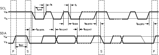 Figure 1. SMBus Timing Diagram
8.6 Switching Characteristics
Unless otherwise stated, the following conditions apply: VVIN = 48 V, –40°C < TJ < 125°C, VUVLO = 3 V , VOVLO = 0 V, RPWR= 20 kΩ.| PARAMETER | CONDITIONS | MIN | TYP | MAX | UNIT | |
|---|---|---|---|---|---|---|
| UVLO/EN, OVLO PINS | ||||||
| UVLODEL | UVLO delay | Delay to GATE high | 7 | 9.6 | 12.2 | µs |
| Delay to GATE low | 6 | 8.5 | 11 | |||
| OVLODEL | OVLO delay | Delay to GATE high | 7 | 9.6 | 12.2 | µs |
| Delay to GATE low | 6 | 8.5 | 11 | |||
| FB PIN | ||||||
| FBDEL | FB Delay | Delay to PGD high | 5 | 7.6 | 10 | µs |
| Delay to PGD low | 7 | 9.2 | 12.5 | |||
| CURRENT LIMIT | ||||||
| tCL | Response time | VIN-SENSE stepped from 0 to 80 mV; CL = GND | 30 | 50 | µs | |
| CIRCUIT BREAKER | ||||||
| tCB | Response time | VIN-SENSE stepped from 0 to 150 mV, time to GATE low, no load | 0.36 | 0.8 | µs | |
| TIMER (TIMER PIN) | ||||||
| tFAULT_DELAY | Fault to GATE low delay | TIMER pin reaches the upper threshold | 12 | µs | ||
8.7 Typical Characteristics
Unless otherwise specified, the following conditions apply: TJ = 25°C, VIN = 48 V. All graphs show junction temperature.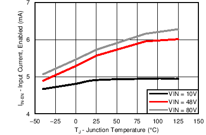
| POR event or CB triggered | ||
| Inject 100 µA into gate node. Measure GATE-SOURCE | ||
| Device Enabled | ||