ZHCSCT1A April 2014 – August 2014 LM5066I
PRODUCTION DATA.
- 1 特性
- 2 应用
- 3 说明
- 4 简化电路原理图
- 5 修订历史记录
- 6 Device Comparison Table
- 7 Pin Configuration and Functions
- 8 Specifications
-
9 Detailed Description
- 9.1 Overview
- 9.2 Functional Block Diagram
- 9.3 Feature Description
- 9.4 Device Functional Modes
- 9.5
Programming
- 9.5.1 PMBus Command Support
- 9.5.2
Standard PMBus Commands
- 9.5.2.1 OPERATION (01h)
- 9.5.2.2 CLEAR_FAULTS (03h)
- 9.5.2.3 CAPABILITY (19h)
- 9.5.2.4 VOUT_UV_WARN_LIMIT (43h)
- 9.5.2.5 OT_FAULT_LIMIT (4Fh)
- 9.5.2.6 OT_WARN_LIMIT (51h)
- 9.5.2.7 VIN_OV_WARN_LIMIT (57h)
- 9.5.2.8 VIN_UV_WARN_LIMIT (58h)
- 9.5.2.9 STATUS_BYTE (78h)
- 9.5.2.10 STATUS_WORD (79h)
- 9.5.2.11 STATUS_VOUT (7Ah)
- 9.5.2.12 STATUS_INPUT (7Ch)
- 9.5.2.13 STATUS_TEMPERATURE (7dh)
- 9.5.2.14 STATUS_CML (7Eh)
- 9.5.2.15 STATUS_OTHER (7Fh)
- 9.5.2.16 STATUS_MFR_SPECIFIC (80h)
- 9.5.2.17 READ_EIN (86h)
- 9.5.2.18 READ_VIN (88h)
- 9.5.2.19 READ_IIN (89h)
- 9.5.2.20 READ_VOUT (8Bh)
- 9.5.2.21 READ_TEMPERATURE_1 (8Dh)
- 9.5.2.22 READ_PIN (97h)
- 9.5.2.23 MFR_ID (99h)
- 9.5.2.24 MFR_MODEL (9Ah)
- 9.5.2.25 MFR_REVISION (9Bh)
- 9.5.3
Manufacturer Specific PMBus Commands
- 9.5.3.1 MFR_SPECIFIC_00: READ_VAUX (D0h)
- 9.5.3.2 MFR_SPECIFIC_01: MFR_READ_IIN (D1h)
- 9.5.3.3 MFR_SPECIFIC_02: MFR_READ_PIN (D2h)
- 9.5.3.4 MFR_SPECIFIC_03: MFR_IN_OC_WARN_LIMIT (D3h)
- 9.5.3.5 MFR_SPECIFIC_04: MFR_PIN_OP_WARN_LIMIT (D4h)
- 9.5.3.6 MFR_SPECIFIC_05: READ_PIN_PEAK (D5h)
- 9.5.3.7 MFR_SPECIFIC_06: CLEAR_PIN_PEAK (D6h)
- 9.5.3.8 MFR_SPECIFIC_07: GATE_MASK (D7h)
- 9.5.3.9 MFR_SPECIFIC_08: ALERT_MASK (D8h)
- 9.5.3.10 MFR_SPECIFIC_09: DEVICE_SETUP (D9h)
- 9.5.3.11 MFR_SPECIFIC_10: BLOCK_READ (DAh)
- 9.5.3.12 MFR_SPECIFIC_11: SAMPLES_FOR_AVG (DBh)
- 9.5.3.13 MFR_SPECIFIC_12: READ_AVG_VIN (DCh)
- 9.5.3.14 MFR_SPECIFIC_13: READ_AVG_VOUT (DDh)
- 9.5.3.15 MFR_SPECIFIC_14: READ_AVG_IIN (DEh)
- 9.5.3.16 MFR_SPECIFIC_14: READ_AVG_PIN (DFh)
- 9.5.3.17 MFR_SPECIFIC_15: READ_AVG_PIN
- 9.5.3.18 MFR_SPECIFIC_16: BLACK_BOX_READ (E0h)
- 9.5.3.19 MFR_SPECIFIC_17: READ_DIAGNOSTIC_WORD (E1h)
- 9.5.3.20 MFR_SPECIFIC_18: AVG_BLOCK_READ (E2h)
- 9.5.4 Reading and Writing Telemetry Data and Warning Thresholds
- 9.5.5 Determining Telemetry Coefficients Empirically With Linear Fit
- 9.5.6 Writing Telemetry Data
- 9.5.7 PMBus Address Lines (ADR0, ADR1, ADR2)
- 9.5.8 SMBA Response
-
10Application and Implementation
- 10.1 Application Information
- 10.2
Typical Application
- 10.2.1
48-V, 10-A PMBus Hotswap Design
- 10.2.1.1 Design Requirements
- 10.2.1.2
Detailed Design-In Procedure
- 10.2.1.2.1 Select RSNS and CL Setting
- 10.2.1.2.2 Selecting the Hotswap FETs
- 10.2.1.2.3 Select Power Limit
- 10.2.1.2.4 Set Fault Timer
- 10.2.1.2.5 Check MOSFET SOA
- 10.2.1.2.6 Set UVLO and OVLO Thresholds
- 10.2.1.2.7 Power Good Pin
- 10.2.1.2.8 Input and Output Protection
- 10.2.1.2.9 Final Schematic and Component Values
- 10.2.1.3 Application Curves
- 10.2.2
48-V, 20-A PMBus Hotswap Design
- 10.2.2.1 Design Requirements
- 10.2.2.2
Detailed Design Procedure
- 10.2.2.2.1 Selecting the Sense Resistor and CL Setting
- 10.2.2.2.2 Selecting the Hotswap FETs
- 10.2.2.2.3 Select Power Limit
- 10.2.2.2.4 Set Fault Timer
- 10.2.2.2.5 Check MOSFET SOA
- 10.2.2.2.6 Switching to dv/dt-Based Start-Up
- 10.2.2.2.7 Choosing the VOUT Slew Rate
- 10.2.2.2.8 Select Power Limit and Fault Timer
- 10.2.2.2.9 Chose Input and Output Protection and Set Undervoltage, Overvoltage, and Power Good Thresholds
- 10.2.2.2.10 Final Schematic and Component Values
- 10.2.2.3 Application Curves
- 10.2.1
48-V, 10-A PMBus Hotswap Design
- 11Power Supply Recommendations
- 12Layout
- 13器件和文档支持
- 14机械封装和可订购信息
12 Layout
12.1 Layout Guidelines
The following guidelines should be followed when designing the PC board for the LM5066I:
- Place the LM5066I close to the board’s input connector to minimize trace inductance from the connector to the MOSFET.
- Place a TVS, Z1, directly adjacent to the VIN and GND pins of the LM5066I to help minimize voltage transients which may occur on the input supply line. The TVS should be chosen such that the peak VIN is just lower the TVS reverse-bias voltage. Transients of 20 V or greater over the nominal input voltage can easily occur when the load current is shut off. A small capacitor may be sufficient for low current sense applications (I < 2 A). TI recommends to test the VIN input voltage transient performance of the circuit by current limiting or shorting the load and measuring the peak input voltage transient.
- Place a 1-µF ceramic capacitor as close as possible to VREF pin.
- Place a 1-µF ceramic capacitor as close as possible to VDD pin.
- The sense resistor (RSNS) should be placed close to the LM5066I. A trace should connect the VIN pad and Q1 pad of the sense resistor to VIN_K and SENSE pins, respectively. Connect RSNS using the Kelvin techniques as shown in Figure 52.
- The high current path from the board’s input to the load (through Q1), and the return path, should be parallel and close to each other to minimize loop inductance.
- The AGND and GND connections should be connected at the pins of the device. The ground connections for the various components around the LM5066I should be connected directly to each other, and to the LM5066I’s GND and AGND pin connection, and then connected to the system ground at one point. Do not connect the various component grounds to each other through the high current ground line.
- Provide adequate thermal sinking for the series pass device (Q1) to help reduce stresses during turn-on and turn-off.
- The board’s edge connector can be designed such that the LM5066I detects through the UVLO/EN pin that the board is being removed, and responds by turning off the load before the supply voltage is disconnected. For example, in Figure 51, the voltage at the UVLO/EN pin goes to ground before VIN is removed from the LM5066I as a result of the shorter edge connector pin. When the board is inserted into the edge connector, the system voltage is applied to the LM5066I’s VIN pin before the UVLO voltage is taken high, thereby allowing the LM5066I to turn on the output in a controlled fashion.
12.2 Layout Example
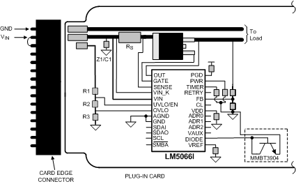 Figure 51. Recommended Board Connector Design
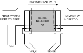 Figure 52. Sense Resistor Connections