ZHCSCT1A April 2014 – August 2014 LM5066I
PRODUCTION DATA.
- 1 特性
- 2 应用
- 3 说明
- 4 简化电路原理图
- 5 修订历史记录
- 6 Device Comparison Table
- 7 Pin Configuration and Functions
- 8 Specifications
-
9 Detailed Description
- 9.1 Overview
- 9.2 Functional Block Diagram
- 9.3 Feature Description
- 9.4 Device Functional Modes
- 9.5
Programming
- 9.5.1 PMBus Command Support
- 9.5.2
Standard PMBus Commands
- 9.5.2.1 OPERATION (01h)
- 9.5.2.2 CLEAR_FAULTS (03h)
- 9.5.2.3 CAPABILITY (19h)
- 9.5.2.4 VOUT_UV_WARN_LIMIT (43h)
- 9.5.2.5 OT_FAULT_LIMIT (4Fh)
- 9.5.2.6 OT_WARN_LIMIT (51h)
- 9.5.2.7 VIN_OV_WARN_LIMIT (57h)
- 9.5.2.8 VIN_UV_WARN_LIMIT (58h)
- 9.5.2.9 STATUS_BYTE (78h)
- 9.5.2.10 STATUS_WORD (79h)
- 9.5.2.11 STATUS_VOUT (7Ah)
- 9.5.2.12 STATUS_INPUT (7Ch)
- 9.5.2.13 STATUS_TEMPERATURE (7dh)
- 9.5.2.14 STATUS_CML (7Eh)
- 9.5.2.15 STATUS_OTHER (7Fh)
- 9.5.2.16 STATUS_MFR_SPECIFIC (80h)
- 9.5.2.17 READ_EIN (86h)
- 9.5.2.18 READ_VIN (88h)
- 9.5.2.19 READ_IIN (89h)
- 9.5.2.20 READ_VOUT (8Bh)
- 9.5.2.21 READ_TEMPERATURE_1 (8Dh)
- 9.5.2.22 READ_PIN (97h)
- 9.5.2.23 MFR_ID (99h)
- 9.5.2.24 MFR_MODEL (9Ah)
- 9.5.2.25 MFR_REVISION (9Bh)
- 9.5.3
Manufacturer Specific PMBus Commands
- 9.5.3.1 MFR_SPECIFIC_00: READ_VAUX (D0h)
- 9.5.3.2 MFR_SPECIFIC_01: MFR_READ_IIN (D1h)
- 9.5.3.3 MFR_SPECIFIC_02: MFR_READ_PIN (D2h)
- 9.5.3.4 MFR_SPECIFIC_03: MFR_IN_OC_WARN_LIMIT (D3h)
- 9.5.3.5 MFR_SPECIFIC_04: MFR_PIN_OP_WARN_LIMIT (D4h)
- 9.5.3.6 MFR_SPECIFIC_05: READ_PIN_PEAK (D5h)
- 9.5.3.7 MFR_SPECIFIC_06: CLEAR_PIN_PEAK (D6h)
- 9.5.3.8 MFR_SPECIFIC_07: GATE_MASK (D7h)
- 9.5.3.9 MFR_SPECIFIC_08: ALERT_MASK (D8h)
- 9.5.3.10 MFR_SPECIFIC_09: DEVICE_SETUP (D9h)
- 9.5.3.11 MFR_SPECIFIC_10: BLOCK_READ (DAh)
- 9.5.3.12 MFR_SPECIFIC_11: SAMPLES_FOR_AVG (DBh)
- 9.5.3.13 MFR_SPECIFIC_12: READ_AVG_VIN (DCh)
- 9.5.3.14 MFR_SPECIFIC_13: READ_AVG_VOUT (DDh)
- 9.5.3.15 MFR_SPECIFIC_14: READ_AVG_IIN (DEh)
- 9.5.3.16 MFR_SPECIFIC_14: READ_AVG_PIN (DFh)
- 9.5.3.17 MFR_SPECIFIC_15: READ_AVG_PIN
- 9.5.3.18 MFR_SPECIFIC_16: BLACK_BOX_READ (E0h)
- 9.5.3.19 MFR_SPECIFIC_17: READ_DIAGNOSTIC_WORD (E1h)
- 9.5.3.20 MFR_SPECIFIC_18: AVG_BLOCK_READ (E2h)
- 9.5.4 Reading and Writing Telemetry Data and Warning Thresholds
- 9.5.5 Determining Telemetry Coefficients Empirically With Linear Fit
- 9.5.6 Writing Telemetry Data
- 9.5.7 PMBus Address Lines (ADR0, ADR1, ADR2)
- 9.5.8 SMBA Response
-
10Application and Implementation
- 10.1 Application Information
- 10.2
Typical Application
- 10.2.1
48-V, 10-A PMBus Hotswap Design
- 10.2.1.1 Design Requirements
- 10.2.1.2
Detailed Design-In Procedure
- 10.2.1.2.1 Select RSNS and CL Setting
- 10.2.1.2.2 Selecting the Hotswap FETs
- 10.2.1.2.3 Select Power Limit
- 10.2.1.2.4 Set Fault Timer
- 10.2.1.2.5 Check MOSFET SOA
- 10.2.1.2.6 Set UVLO and OVLO Thresholds
- 10.2.1.2.7 Power Good Pin
- 10.2.1.2.8 Input and Output Protection
- 10.2.1.2.9 Final Schematic and Component Values
- 10.2.1.3 Application Curves
- 10.2.2
48-V, 20-A PMBus Hotswap Design
- 10.2.2.1 Design Requirements
- 10.2.2.2
Detailed Design Procedure
- 10.2.2.2.1 Selecting the Sense Resistor and CL Setting
- 10.2.2.2.2 Selecting the Hotswap FETs
- 10.2.2.2.3 Select Power Limit
- 10.2.2.2.4 Set Fault Timer
- 10.2.2.2.5 Check MOSFET SOA
- 10.2.2.2.6 Switching to dv/dt-Based Start-Up
- 10.2.2.2.7 Choosing the VOUT Slew Rate
- 10.2.2.2.8 Select Power Limit and Fault Timer
- 10.2.2.2.9 Chose Input and Output Protection and Set Undervoltage, Overvoltage, and Power Good Thresholds
- 10.2.2.2.10 Final Schematic and Component Values
- 10.2.2.3 Application Curves
- 10.2.1
48-V, 10-A PMBus Hotswap Design
- 11Power Supply Recommendations
- 12Layout
- 13器件和文档支持
- 14机械封装和可订购信息
10 Application and Implementation
10.1 Application Information
The LM5066I is a hotswap with a PMBus interface that provides current, voltage, power, and status information to the host. As a hotswap, it is used to manage inrush current and protect in case of faults.
When designing a hotswap, three key scenarios should be considered:
- Start-up
- Output of a hotswap is shorted to ground when the hotswap is on. This is often referred to as a hot-short.
- Powering-up a board when the output and ground are shorted. This is usually called a start-into-short.
All of these scenarios place a lot of stress on the hotswap MOSFET and take special care when designing the hotswap circuit to keep the MOSFET within its SOA. Detailed design examples are provided in the following sections. Solving all of the equations by hand is cumbersome and can result in errors. Instead, TI recommends to use the LM5066I Design Calculator provided on the product page.
10.2 Typical Application
This section shows two application examples. The requirements are the same, except the second design requires twice the current and twice the output capacitance. In the 20A design example, a regular design is attempted using a power limiting based start-up. Unfortunately this results in insufficient margin and the final design relies on a dv/dt based start-up.
10.2.1 48-V, 10-A PMBus Hotswap Design
This section describes the design procedure for a 48-V, 10-A PMBUS hotswap design.
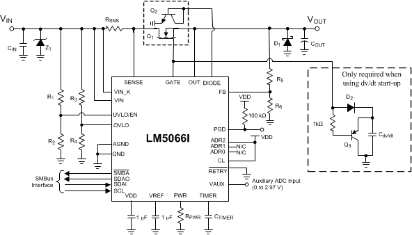 Figure 19. Typical Application Circuit
10.2.1.1 Design Requirements
Table 51 summarizes the design parameters that must be known before designing a hotswap circuit. When charging the output capacitor through the hotswap MOSFET, the FET’s total energy dissipation equals the total energy stored in the output capacitor (1 / 2CV2). Thus, both the input voltage and output capacitance determine the stress experienced by the MOSFET. The maximum load current drives the current limit and sense resistor selection. In addition, the maximum load current, maximum ambient temperature, and thermal properties of the PCB (RθCA) drive the selection of the MOSFET RDSON and the number of MOSFETs used. RθCA is a strong function of the layout and the amount of copper that is connected to the drain of the MOSFET. Note that the drain is not electrically connected to the ground plane, and thus the ground plane cannot be used to help with heat dissipation. This design example uses RθCA = 30°C/W, which is similar to the LM5066I EVM. It is a good practice to measure the RθCA of a given design after the physical PCBs are available.
Finally, it is important to understand what test conditions the hotswap needs to pass. In general, a hotswap is designed to pass both a hot-short and a start into a short, which are described in the previous section. Also, TI recommends to keep the load OFF until the hotswap is fully powered-up. Starting the load early causes unnecessary stress on the MOSFET and could lead to MOSFET failures or a failure to start-up.
Table 51. Design Parameters
| PARAMETER | EXAMPLE VALUE |
|---|---|
| Input voltage range | 40 to 60 V |
| Maximum load current | 10 A |
| Maximum output capacitance of the hotswap | 220 µF |
| Maximum ambient temperature | 85°C |
| MOSFET RθCA (function of layout) | 30°C/W |
| Pass hot-short on output? | Yes |
| Pass a start into short? | Yes |
| Is the load off until PG asserted? | Yes |
| Can a hot board be plugged back in? | Yes |
10.2.1.2 Detailed Design-In Procedure
10.2.1.2.1 Select RSNS and CL Setting
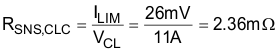
LM5066I can be used with a VCL of 26 or 50 mV. Using the 26-mV threshold results in a lower RSNS and lower I2R losses. The 26-mV option is selected for this design by connecting the CL pin directly to VDD. TI recommends to target a current limit that is at least 10% above the maximum load current to account for the tolerance of the LM5066I current limit. Targeting a current limit of 11 A, the sense resistor can be computed as follows:
Typically, sense resistors are only available in discrete values. If a precise current limit is desired, a sense resistor along with a resistor divider can be used as shown in Figure 20.
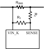 Figure 20. SENSE Resistor Divider
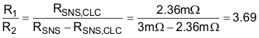
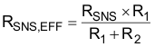
The next larger available sense resistor should be chosen (3 mΩ in this case). The ratio of R1 and R2 can be computed as follows:
Note that the SENSE pin pulls 25 μA of current, which creates an offset across R2. TI recommends to keep R2 below 10 Ω to reduce the offset that this introduces. In addition, the 1% resistors add to the current monitoring error. Finally, if the resistor divider approach is used, the user should compute the effective sense resistance (RSNS,EFF) using Equation 9 and use that in all equations instead of RSNS.
Note that for many applications, a precise current limit may not be required. In that case, it is simpler to pick the next smaller available sense resistor. For this application, a 2-mΩ resistor can be used for a 13-A current limit.
10.2.1.2.2 Selecting the Hotswap FETs
It is critical to select the correct MOSFET for a hotswap design. The device must meet the following requirements:
- The VDS rating should be sufficient to handle the maximum system voltage along with any ringing caused by transients. For most 48-V systems, a 100-V FET is a good choice.
- The SOA of the FET should be sufficient to handle all usage cases: start-up, hot-short, and start into short.
- RDSON should be sufficiently low to maintain the junction and case temperature below the maximum rating of the FET. In fact, TI recommends to keep the steady-state FET temperature below 125°C to allow margin to handle transients.
- Maximum continuous current rating should be above the maximum load current and the pulsed-drain current must be greater than the current threshold of the circuit breaker. Most MOSFETs that pass the first three requirements also pass these two.
- A VGS rating of ±20 V is required because the LM5066I can pull up the gate as high as 16 V above source.
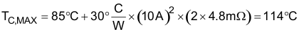
For this design, the PSMN4R8-100BSE was selected for its low RDSON and superior SOA. After selecting the MOSFET, the maximum steady-state case temperature can be computed as follows:

Note that the RDSON is a strong function of junction temperature, which for most D2PACK MOSFETs is very close to the case temperature. A few iterations of the previous equations may be necessary to converge on the final RDSON and TC,MAX value. According to the PSMN4R8-100BSE data sheet, it's RDSON doubles at 110°C. Equation 11 uses this RDSON value to compute the TC,MAX. Note that the computed TC,MAX is close to the junction temperature assumed for RDSON. Thus, no further iterations are necessary.
10.2.1.2.3 Select Power Limit
In general, a lower power limit setting is preferred to reduce the stress on the MOSFET. However, when the LM5066I is set to a very-low power limit setting, it has to regulate the FET current and hence the voltage across the sense resistor (VSNS) to a very-low value. VSNS can be computed as shown in Equation 12.

To avoid significant degradation of the power limiting, TI does not recommend a VSNS of less than 4 mV. Based on this requirement, the minimum allowed power limit can be computed as follows:
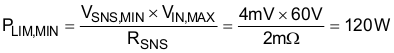
In most applications, the power limit can be set to PLIM,MIN using Equation 14. Here RSNS and RPWR are in ohms and PLIM is in watts.
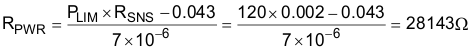
The closest available resistor should be selected. In this case, a 28.2-kΩ resistor was chosen.
10.2.1.2.4 Set Fault Timer
The fault timer runs when the hotswap is in power limit or current limit, which is the case during start-up. Thus, the timer has to be sized large enough to prevent a time-out during start-up. If the part starts directly into current limit (ILIM × VDS < PLIM), the maximum start time can be computed with Equation 15.
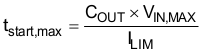
For most designs (including this example), ILIM × VDS > PLIM, so the hotswap starts in power limit and transitions into current limit. In that case, the maximum start time can be computed as in Equation 16.
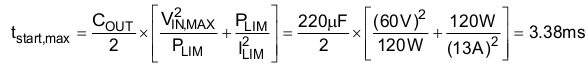
Note that the above start-time is based on typical current limit and power limit values. To ensure that the timer never times out during start-up, TI recommends to set the fault time (tflt) to be 1.5 × tstart,max or 5.1 ms. This accounts for the variation in power limit, timer current, and timer capacitance. Thus, CTIMER can be computed as follows:
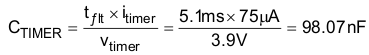
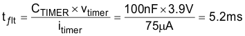
The next largest standards capacitor value for CTIMER is chosen as 100 nF. After CTIMER is chosen, the actual programmed fault time can be computed as follows:
10.2.1.2.5 Check MOSFET SOA
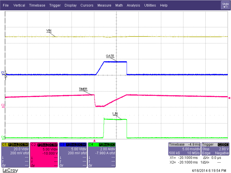
When the power limit and fault timer are chosen, it is critical to check that the FET stays within its SOA during all test conditions. During a hot-short the circuit breaker trips and the LM5066I restarts into power limit until the timer runs out. In the worst case, the MOSFET’s VDS equals VIN,MAX, IDS equals PLIM / VIN,MAX and the stress event lasts for tflt. For this design example, the MOSFET has 60 V, 2 A across it for 5.2 ms.
Based on the SOA of the PSMN4R8-100BSE, it can handle 60 V, 30 A for 1 ms and it can handle 60 V, 6 A for 10 ms. For 5.2 ms, the SOA can be extrapolated by approximating SOA versus time as a power function as shown below:
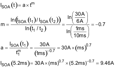
Note that the SOA of a MOSFET is specified at a case temperature of 25°C, while the case temperature can be much hotter during a hot-short. The SOA should be de-rated based on TC,MAX using Equation 20:

Based on this calculation, the MOSFET can handle 3.85 A, 60 V for 5.2 ms at elevated case temperature, but is only required to handle 2 A during a hot-short. Thus, there is good margin and the design is robust. In general, TI recommends that the MOSFET can handle 1.3× more than what is required during a hot-short. This provides margin to account for the variance of the power limit and fault time.
10.2.1.2.6 Set UVLO and OVLO Thresholds
By programming the UVLO and OVLO thresholds, the LM5066I enables the series-pass device (Q1) when the input supply voltage (VIN) is within the desired operational range. If VIN is below the UVLO threshold or above the OVLO threshold, Q1 is switched off, denying power to the load. Hysteresis is provided for each threshold.
10.2.1.2.6.1 Option A
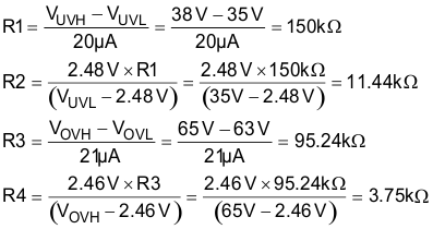
The configuration shown in Figure 21 requires three resistors (R1 to R3) to set the thresholds.
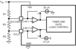 Figure 21. UVLO And OVLO Thresholds Set By R1-R3
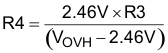
The procedure to calculate the resistor values is as follows:
- Choose the upper UVLO threshold (VUVH) and the lower UVLO threshold (VUVL).
- Choose the upper OVLO threshold (VOVH).
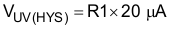
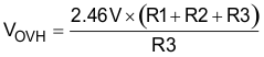
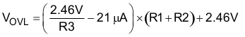
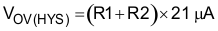
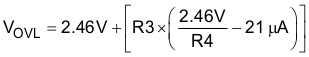
- The lower OVLO threshold (VOVL) cannot be chosen in advance in this case, but is determined after the values for R1 to R3 are determined. If VOVL must be accurately defined in addition to the other three thresholds, see Option B. The resistors are calculated as follows:
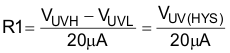
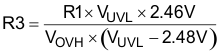
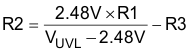
The lower OVLO threshold is calculated from:
When the R1 to R3 resistor values are known, the threshold voltages and hysteresis are calculated from the following:
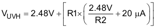
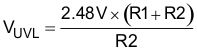
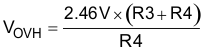
10.2.1.2.6.2 Option B
If all four thresholds must be accurately defined, the configuration in Figure 22 can be used.
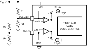 Figure 22. Programming the Four Thresholds
The four resistor values are calculated as follows:
- Choose the upper and lower UVLO thresholds (VUVH) and (VUVL).
- Choose the upper and lower OVLO threshold (VOVH) and (VOVL).
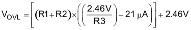
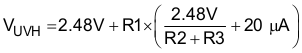
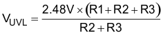
- When the R1 to R4 resistor values are known, the threshold voltages and hysteresis are calculated from the following:

10.2.1.2.6.3 Option C
The minimum UVLO level is obtained by connecting the UVLO/EN pin to VIN as shown in Figure 23. Q1 is switched on when the VIN voltage reaches the POREN threshold (≊8.6 V). The OVLO thresholds are set using R3, R4. Their values are calculated using the procedure in Option B.
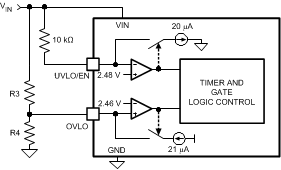 Figure 23. UVLO = POREN
10.2.1.2.6.4 Option D
The OVLO function can be disabled by grounding the OVLO pin. The UVLO thresholds are set as described in Option B or Option C.
For this design example, option B was used and the following options were targeted: VUVH = 38 V, VUVL = 35 V, VOVH = 65 V, and VOVL = 63 V. The VUVH and VOVL were chosen to be 5% below or above the input voltage range of 40 to 60 V to allow for some tolerance in the thresholds of the part. R1, R2, R3, and R4 are computed using the following equations:
Nearest available 1% resistors should be chosen. Set R1 = 150 kΩ, R2 = 11.5 kΩ, R3 = 95.3 kΩ, and R4 = 3.74 kΩ.
10.2.1.2.7 Power Good Pin
The Power Good indicator pin (PGD) is connected to the drain of an internal N-channel MOSFET capable of sustaining 80 V in the off-state and transients up to 100 V. An external pullup resistor is required at PGD to an appropriate voltage to indicate the status to downstream circuitry. The off-state voltage at the PGD pin can be higher or lower than the voltages at VIN and OUT. PGD is switched high when the voltage at the FB pin exceeds the PGD threshold voltage. Typically, the output voltage threshold is set with a resistor divider from output to feedback, although the monitored voltage need not be the output voltage. Any other voltage can be monitored as long as the voltage at the FB pin does not exceed its maximum rating. Referring to the Functional Block Diagram, when the voltage at the FB pin is below its threshold, the 20-µA current source at FB is disabled. As the output voltage increases, taking FB above its threshold, the current source is enabled, sourcing current out of the pin, raising the voltage at FB to provide threshold hysteresis. The PGD output is forced low when either the UVLO/EN pin is below its threshold or the OVLO pin is above its threshold. The status of the PGD pin can be read through the PMBus interface in either the STATUS_WORD (79h) or DIAGNOSTIC_WORD (E1h) registers.
When the voltage at the FB pin increases above its threshold, the internal pulldown acting on the PGD pin is disabled allowing PGD to rise to VPGD through the pullup resistor, RPG, as shown in Figure 25. The pullup voltage (VPGD) can be as high as 80 V, and can be higher or lower than the voltages at VIN and OUT. VDD is a convenient choice for VPGD as it allows interface to low voltage logic and avoids glitching on PGD during power-up. If a delay is required at PGD, suggested circuits are shown in Figure 26. In Figure 26(A), capacitor CPG adds delay to the rising edge, but not to the falling edge. In Figure 26(B), the rising edge is delayed by RPG1 + RPG2 and CPG, while the falling edge is delayed a lesser amount by RPG2 and CPG. Adding a diode across RPG2 (Figure 26(C)) allows for equal delays at the two edges, or a short delay at the rising edge and a long delay at the falling edge.
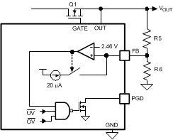 Figure 24. Programming the PGD Threshold
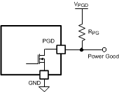 Figure 25. Power Good Output
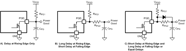 Figure 26. Adding Delay to the Power Good Output Pin
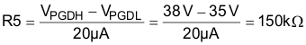
TI recommends to set the PG threshold 5% below the minimum input voltage to ensure that the PG is asserted under all input voltage conditions. For this example, PGDH of 38 V and PGDL of 35 V is targeted. R5 and R6 are computed using the following equations:
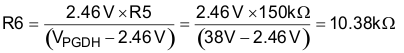
Nearest available 1% resistors should be chosen. Set R5 = 150 kΩ and R6 = 10.5 kΩ.
10.2.1.2.8 Input and Output Protection
Proper operation of the LM5066I hot swap circuit requires a voltage clamping element present on the supply side of the connector into which the hot swap circuit is plugged in. A TVS is ideal, as depicted in Figure 27. The TVS is necessary to absorb the voltage transient generated whenever the hot swap circuit shuts off the load current. This effect is the most severe during a hot-short when a large current is suddenly interrupted when the FET shutts off. The TVS should be chosen to have minimal leakage current at VIN,MAX and to clamp the voltage to under 100V during hot-short events. For many high power applications 5.0SMDJ60A is a good choice.
If the load powered by the LM5066I hot swap circuit has inductive characteristics, a Schottky diode is required across the LM5066I’s output, along with some load capacitance. The capacitance and the diode are necessary to limit the negative excursion at the OUT pin when the load current is shut off.
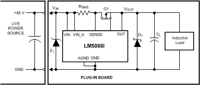 Figure 27. Output Diode Required for Inductive Loads
10.2.1.2.9 Final Schematic and Component Values
Figure 19 shows the schematic used to implement the requirements described in the previous section. In addition, Table 52 provides the final component values that were used to meet the design requirements for a 48-V, 10-A hotswap design. The application curves in the next section are based on these component values.
Table 52. Final Component Values (48-V, 10-A Design)
| COMPONENT | VALUE | |
|---|---|---|
| RSNS | 2 mΩ | |
| R1 | 150 kΩ | |
| R2 | 11.5 kΩ | |
| R3 | 95.3 kΩ | |
| R4 | 3.74 kΩ | |
| R5 | 150 kΩ | |
| R6 | 10.5 kΩ | |
| RPWR | 28.2 kΩ | |
| Q1 | PSMN4R8-100BSEJ | |
| Q2 | MMBT3904 | |
| D1 | B380-13-F | |
| Z1 | 5.0SMDJ60A | |
| CTIMER | 100 nF | |
| Optional dv/dt circuit | DNP | |
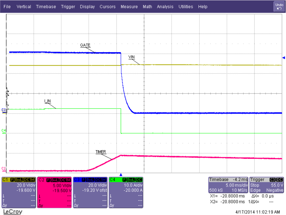
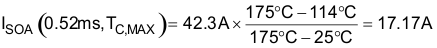
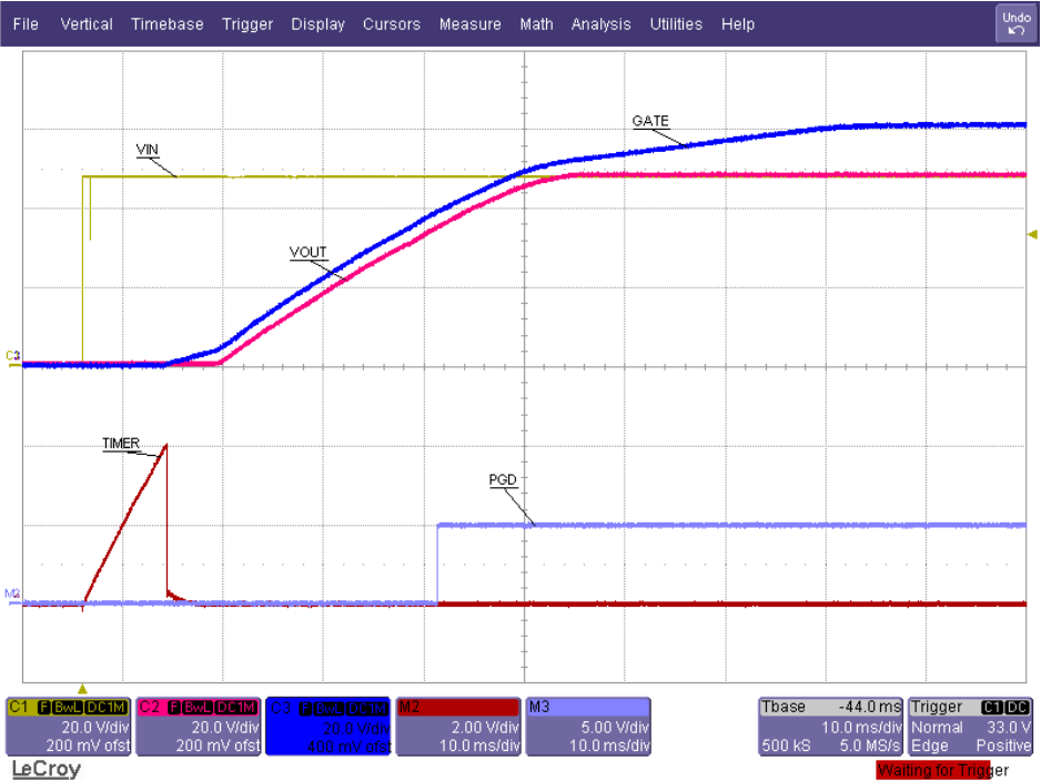
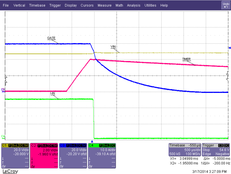
10.2.1.3 Application Curves
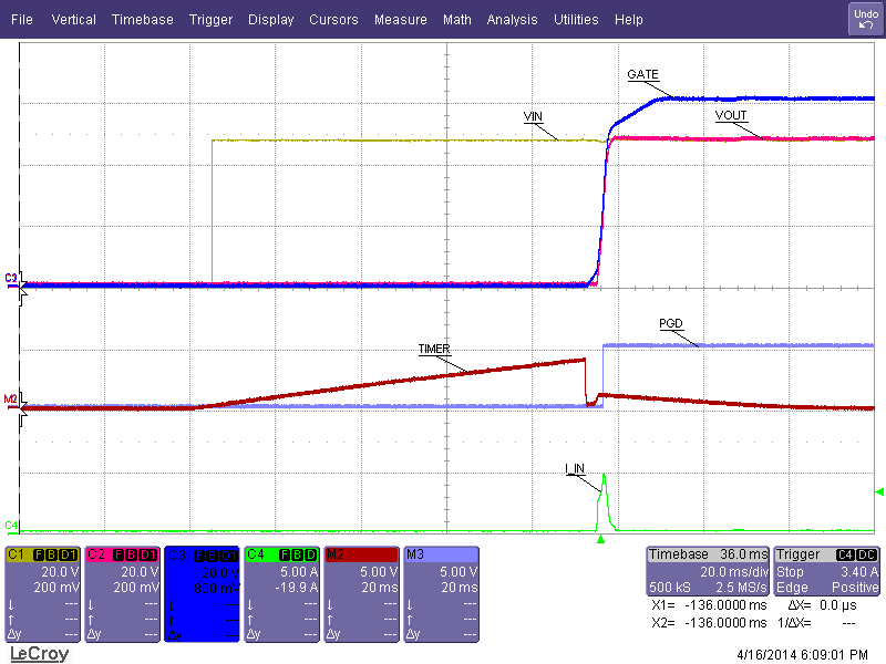
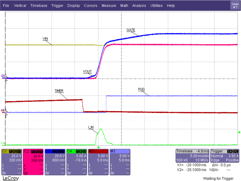
| VIN = 40 V |
_10A_snvs950.png)

| VIN = 48 V |
| VIN = 60 V |
_10A_snvs950.png)
10.2.2 48-V, 20-A PMBus Hotswap Design
This section describes the design procedure for a 48-V, 20-A PMBUS hotswap design.
Figure 40. Typical Application Schematic, LM5066I
10.2.2.1 Design Requirements
Table 53. Design Parameters
| PARAMETER | EXAMPLE VALUE |
|---|---|
| Input voltage range | 40 to 60 V |
| Maximum load current | 20 A |
| Maximum output capacitance of the hotswap | 440 µF |
| Maximum ambient temperature | 85°C |
| MOSFET RθCA (function of layout) | 30°C/W |
| Pass hot-short on output? | Yes |
| Pass a start into short? | Yes |
| Is the load off until PG asserted? | Yes |
| Can a hot board be plugged back in? | Yes |
10.2.2.2 Detailed Design Procedure
10.2.2.2.1 Selecting the Sense Resistor and CL Setting
LM5066I can be used with a VCL of 26 or 50 mV. In general using the 26-mV threshold results in a lower RSNS and lower I2R losses. This option is selected for this design by connecting the CL pin directly to VDD. TI recommends to target a current limit that is at least 10% above the maximum load current to account for the tolerance of the LM5066I current limit. Targeting a current limit of 22 A, the sense resistor can be computed as follows:
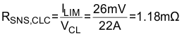
For this application, a 1-mΩ resistor can be used for a 26-A current limit.
10.2.2.2.2 Selecting the Hotswap FETs
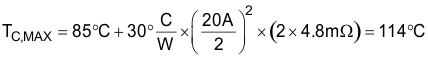
For this design, the PSMN4R8-100BSE was selected for its low RDSON and superior SOA. After selecting the MOSFET, the maximum steady-state case temperature can be computed as follows:

Note that the RDSON is a strong function of junction temperature, which for most D2PACK MOSFETs are very close to the case temperature. A few iterations of the previous equations may be necessary to converge on the final RDSON and TC,MAX value. According to the PSMN4R8-100BSE data sheet, its RDSON doubles at 110°C. Equation 45 uses this RDSON value to compute the TC,MAX. Note that the computed TC,MAX is already above the absolute maximum of the FET.
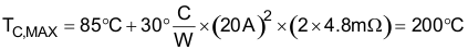
This suggests that two FETs should be used for the design. During steady-state operation, the MOSFETs are fully enhanced and share current evenly. Thus, assuming that each FET carries half of the current, the TC,MAX can be computed with Equation 46. Now TC,MAX is 114°C, which is reasonable.
10.2.2.2.3 Select Power Limit
In general, a lower power limit setting is preferred to reduce the stress on the MOSFET. However, when the LM5066I is set to a very-low power limit setting, it has to regulate the FET current and hence the voltage across the sense resistor (VSNS) to a very-low value. VSNS can be computed as shown in Equation 47.
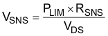
To avoid significant degradation of the power limiting, TI does not recommend a VSNS below 4 mV. Based on this requirement, the minimum allowed power limit can be computed as follows:
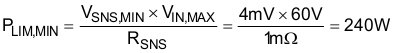
In most applications, the power limit can be set to PLIM,MIN as shown. Here RSNS and RPWR are in ohms and PLIM is in watts.
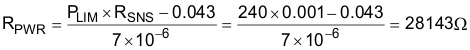
The closest available resistor should be selected. In this case a 28.2-kΩ resistor was chosen.
10.2.2.2.4 Set Fault Timer
The maximum start time can be computed to 3.37 ms as shown in Equation 50.
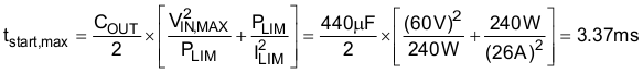
Note this start-time is based on typical current limit and power limit values. To ensure that the timer never times out during start-up, TI recommends to set the fault time (TFLT) to be 1.5× tstart,max or 5.1 ms. This accounts for the variation in power limit, timer current, and timer capacitance. Thus, CTIMER can be computed as follows:
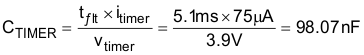
The next largest available CTIMER is chosen as 100 nF. After CTIMER is chosen, the actual programmed fault time can be computed as follows:

10.2.2.2.5 Check MOSFET SOA
After the power limit and fault timer are chosen, it is critical to check that the FET stays within its SOA during all test conditions. During a hot-short, the circuit breaker trips and the LM5066I restarts into power limit until the timer runs out. In the worst case, the MOSFET’s VDS equals VIN,MAX, IDS equals PLIM / VIN,MAX, and the stress event lasts for tflt. For this design example, the MOSFET has 60 V, 4 A across it for 5.2 ms.
When the hotswap is in power limit and the FETs are operating in saturation region (VGS close to threshold voltage), the designer cannot assume that the FETs will share. Even a small VT mismatch causes a large difference in the current carried by the two MOSFETs. Thus, the SOA checking should be done assuming that all of the current is flowing through a single FET.
Based on the SOA of the PSMN4R8-100BSE, it can handle 60 V, 30 A for 1 ms and it can handle 60 V, 6 A for 10 ms. The SOA for 5.2 ms can be extrapolated by approximating SOA versus time as a power function as shown in the following equations:
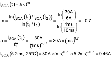
Note that the SOA of a MOSFET is specified at a case temperature of 25°C, while the case temperature can be much hotter during a hot-short. The SOA should be de-rated based on TC,MAX using Equation 54.

Based on this calculation, the MOSFET can handle 3.85 A, 60 V for 5.2 ms at elevated case temperature, but it is required to handle 4 A during a hot-short. In addition, there is tolerance on the power limit and timer, so using these settings would not produce a robust hotswap design.
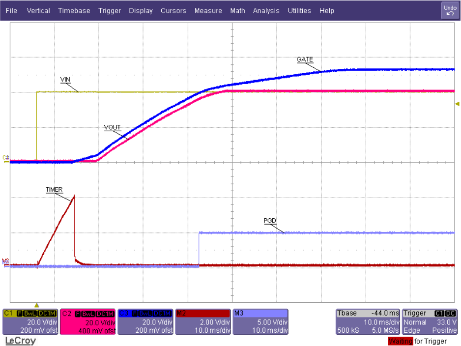
10.2.2.2.6 Switching to dv/dt-Based Start-Up
For designs with large load currents and output capacitances, using a power-limit-based start-up can be impractical. Fundamentally, increasing load currents reduces the sense resistor, which increases the minimum power limit. Using a larger output capacitor results in a longer start-up time and requires a longer timer. Thus, a longer timer and a larger power limit setting is required, which places more stress on the MOSFET during a hot-short or a start into short. Eventually, there will be no FETs that can support such a requirement.
To avoid this problem, a dv/dt limiting capacitor (Cdv/dt) can be used to limit the slew rate of the gate and the output voltage. The inrush current can be set arbitrarily small by reducing the slew rate of VOUT. In addition, the power limit is set to satisfy the minimum power limit requirement and to keep the timer from running during start-up (make PLIM / VINMAX > IINR). Because the timer does not run during start-up, it can be made arbitrarily small to reduce the stress that the MOSFET experiences during a start into short or a hot-short.
The D2 prevents the charge of Cdv/dt from interfering with the power limit loop during a hot-short event and Q3 discharges Cdv/dt when the hotswap gate comes down.
10.2.2.2.7 Choosing the VOUT Slew Rate
The inrush current should be kept low enough to keep the MOSFET within its SOA during start-up. Note that the total energy dissipated in the MOSFET during start-up is constant regardless of the inrush time. Thus, stretching it out over a longer time always reduces the stress on the MOSFET as long as the load is off during start-up.
When choosing a target slew rate, one should pick a reasonable number, check the SOA, and reduce the slew rate if necessary. Using 4 V/ms as a starting point, the inrush current can be computed as follows:
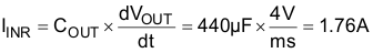
Assuming a maximum input voltage of 60 V, it takes 15 ms to start-up. Note that the power dissipation of the FET starts at VIN,MAX × IINR and reduce to 0 as the VDS of the MOSFET is reduced. Note that the SOA curves assume the same power dissipation for a given time. A conservative approach is to assume an equivalent power profile where PFET = VIN,MAX × IINR for t = tstart-up / 2. In this instance, the SOA can be checked by looking at a 60-V, 1.76-A, 7.5-ms pulse. Using the same technique as section Check MOSFET SOA, the MOSFET SOA can be estimated as follows:

This value has to also be derated for temperature. For this calculation, it is assumed that TC can equal TC,MAX when the board is plugged in. This would only occur if a hot board is unplugged, then plugged back in before it cools off. This is worst case and for many applications, the TA,MAX can be used for this derating.

This calculation shows that the MOSFET stays well-within its SOA during a start-up if the slew rate is 4 V/ms. Note that if the load is off during start-up, the total energy dissipated in the FET is constant regardless of the slew rate. Thus, a lower slew rate always places less stress on the FET. To ensure that the slew rate is at most 4 V/ms, the Cdv/dt should be chosen as follows:
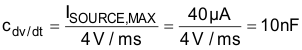
Next, the typical slew rate and start time can be computed to be 2 V/ms as shown in Equation 59, making the typical start time 30 ms.
10.2.2.2.8 Select Power Limit and Fault Timer
When picking the power limit it needs to meet two requirements:
- Power limit is large enough to avoid operating with VSNS < 4 mV
- Power limit is large enough to ensure that the timer does not run during start up. Picking a power limit such that it is 2× of IINR,MAX × VIN,MAX is good practice.
Thus, the minimum allowed power limit can be computed as follows:

Next, the power limit is set to PLIM,MIN using Equation 61. Here RSNS and RPWR are in ohms and PLIM is in watts.
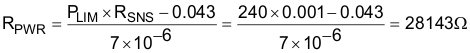
The closest available resistor should be selected. In this case, a 28.2-kΩ resistor was chosen.
Next, a fault timer value should be selected. In general, the timer value should be decreased until there is enough margin between available SOA and the power pulse the FET experiences during a hot-short. For this design, a 10-nF CTIMER was chosen corresponding to a 520 µs. The available SOA is extrapolated using the method described earlier.
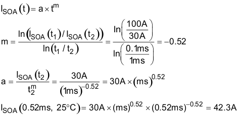
Next, the available SOA is derated for temperature:
Note that only 4 A was required, while the FET can support 17.17 A. This confirms that the design is robust and has plenty of margin.
10.2.2.2.9 Chose Input and Output Protection and Set Undervoltage, Overvoltage, and Power Good Thresholds
This is identical to the previous design. Refer to Set UVLO and OVLO Thresholds, Power Good Pin, and Input and Output Protection for these settings.
10.2.2.2.10 Final Schematic and Component Values
Figure 40 shows the schematic used to implement the requirements described in the 48-V, 20-A PMBus Hotswap Design section. In addition, Table 54 provides the final component values used to meet the design requirements for a 48-V, 20-A hotswap design. The application curves in the next section are based on these components.
Table 54. Final Component Values (48-V, 20-A Design)
| Component | Value | |
|---|---|---|
| RSNS | 1 mΩ | |
| R1 | 150 kΩ | |
| R2 | 11.5 kΩ | |
| R3 | 95.3 kΩ | |
| R4 | 3.74 kΩ | |
| R5 | 150 kΩ | |
| R6 | 10.5 kΩ | |
| RPWR | 28.2 kΩ | |
| Q1 | 2x (PSMN4R8-100BSEJ) | |
| Q2 | MMBT3904 | |
| D1 | B380-13-F | |
| Z1 | 5.0SMDJ60A | |
| CTIMER | 10 nF | |
| Optional dv/dt circuit | Yes | |
| D2 | 1N4148W-7-F | |
| Q3 | MMBT5401LT1G | |
| Cdvdt | 10 nF | |
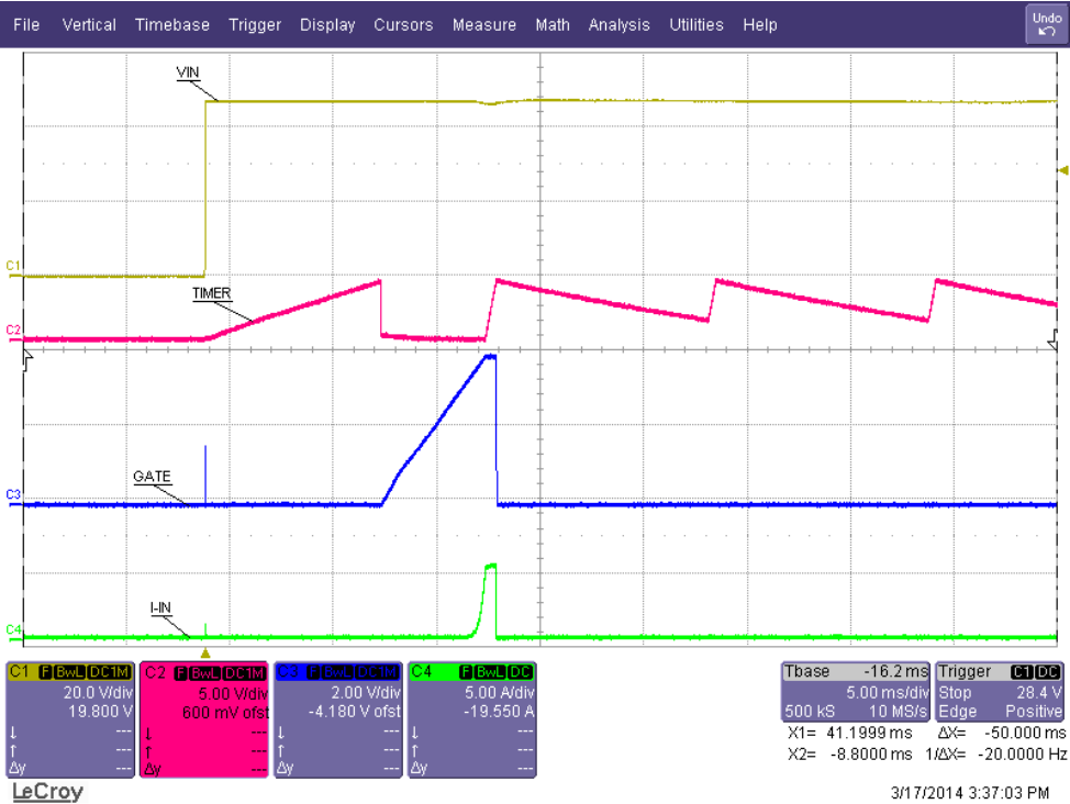
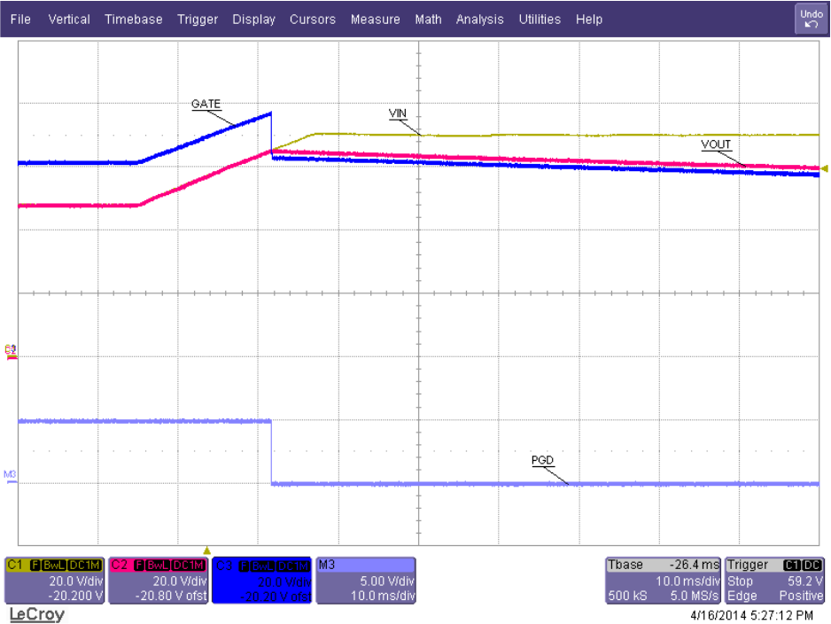
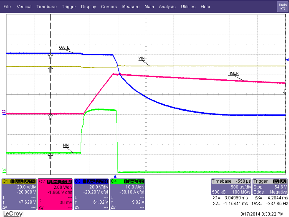
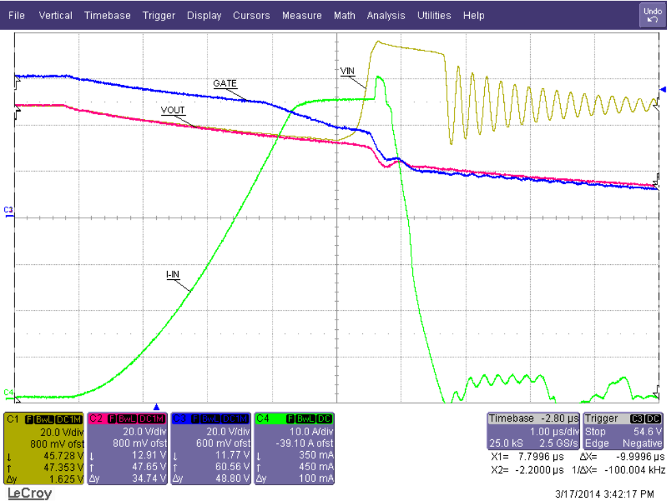
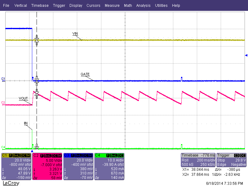
10.2.2.3 Application Curves
| VIN = 48 V |
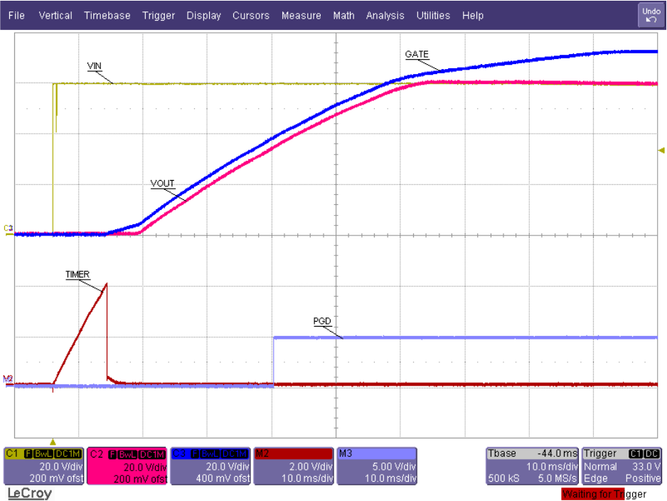
| VIN = 60 V |
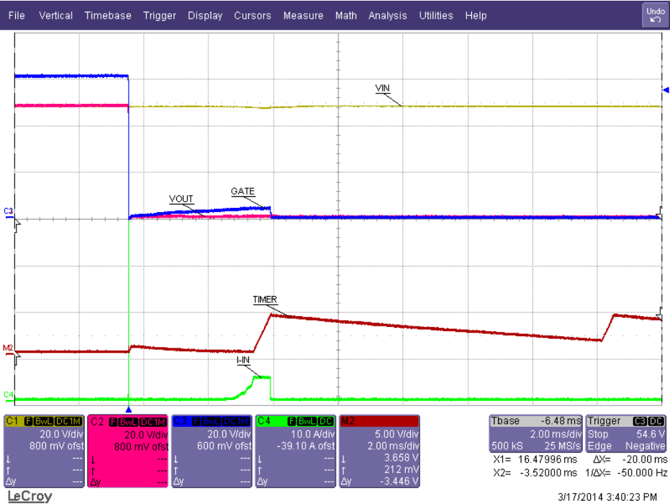
| VIN = 40 V |