ZHCSHC6I January   2007  – December 2017 LM5022

PRODUCTION DATA.  

  1. 特性
  2. 应用
  3. 说明
    1.     Device Images
      1.      典型应用
  4. 修订历史记录
  5. Pin Configuration and Functions
    1.     Pin Functions
  6. Specifications
    1. 6.1 Absolute Maximum Ratings
    2. 6.2 ESD Ratings
    3. 6.3 Recommended Operating Conditions
    4. 6.4 Thermal Information
    5. 6.5 Electrical Characteristics
    6. 6.6 Typical Characteristics
  7. Detailed Description
    1. 7.1 Overview
    2. 7.2 Functional Block Diagram
    3. 7.3 Feature Description
      1. 7.3.1 High-Voltage Start-Up Regulator
      2. 7.3.2 Input Undervoltage Detector
      3. 7.3.3 Error Amplifier
      4. 7.3.4 Current Sensing and Current Limiting
      5. 7.3.5 PWM Comparator and Slope Compensation
      6. 7.3.6 Soft Start
      7. 7.3.7 MOSFET Gate Driver
      8. 7.3.8 Thermal Shutdown
    4. 7.4 Device Functional Modes
      1. 7.4.1 Oscillator, Shutdown, and SYNC
  8. Application and Implementation
    1. 8.1 Application Information
    2. 8.2 Typical Application
      1. 8.2.1 Design Requirements
      2. 8.2.2 Detailed Design Procedure
        1. 8.2.2.1  Switching Frequency
        2. 8.2.2.2  MOSFET
        3. 8.2.2.3  Output Diode
        4. 8.2.2.4  Boost Inductor
        5. 8.2.2.5  Output Capacitor
        6. 8.2.2.6  VCC Decoupling Capacitor
        7. 8.2.2.7  Input Capacitor
        8. 8.2.2.8  Current Sense Filter
        9. 8.2.2.9  RSNS, RS2 and Current Limit
        10. 8.2.2.10 Control Loop Compensation
        11. 8.2.2.11 Efficiency Calculations
          1. 8.2.2.11.1 Chip Operating Loss
          2. 8.2.2.11.2 MOSFET Switching Loss
          3. 8.2.2.11.3 MOSFET and RSNS Conduction Loss
          4. 8.2.2.11.4 Output Diode Loss
          5. 8.2.2.11.5 Input Capacitor Loss
          6. 8.2.2.11.6 Output Capacitor Loss
          7. 8.2.2.11.7 Boost Inductor Loss
          8. 8.2.2.11.8 Total Loss
          9. 8.2.2.11.9 Efficiency
      3. 8.2.3 Application Curves
  9. Power Supply Recommendations
  10. 10Layout
    1. 10.1 Layout Guidelines
      1. 10.1.1 Filter Capacitors
      2. 10.1.2 Sense Lines
      3. 10.1.3 Compact Layout
      4. 10.1.4 Ground Plane and Shape Routing
    2. 10.2 Layout Examples
  11. 11器件和文档支持
    1. 11.1 器件支持
      1. 11.1.1 第三方产品免责声明
      2. 11.1.2 设计支持
    2. 11.2 文档支持
      1. 11.2.1 相关文档
    3. 11.3 接收文档更新通知
    4. 11.4 社区资源
    5. 11.5 商标
    6. 11.6 静电放电警告
    7. 11.7 Glossary
  12. 12机械、封装和可订购信息

封装选项

机械数据 (封装 | 引脚)
散热焊盘机械数据 (封装 | 引脚)
订购信息

Application Curves

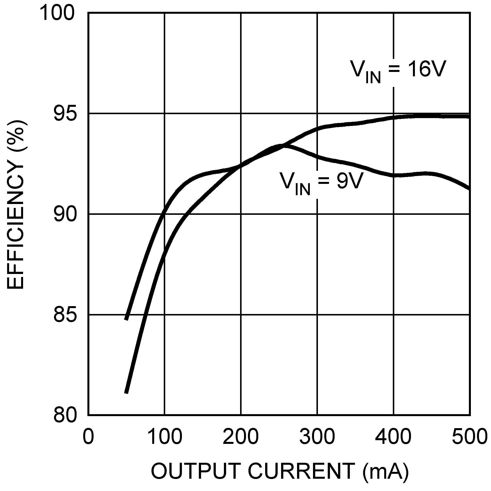
LM5022 Figure 15.png
Figure 22. Efficiency
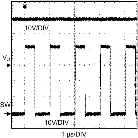
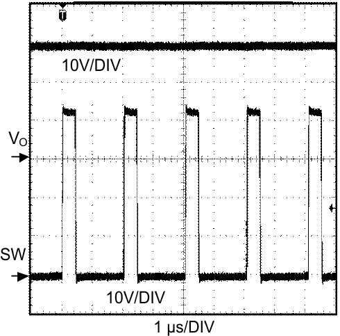
LM5022 Figure_17.gif
VIN = 16 V, IO = 0.5 A
Figure 24. Switch Node Voltage
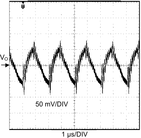
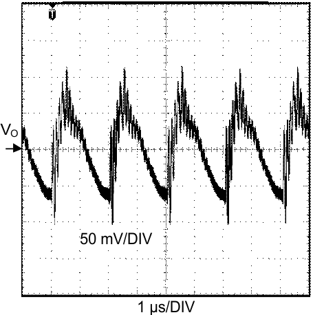
LM5022 Figure_19.gif
VIN = 16 V, IO = 0.5 A
Figure 26. Output Voltage Ripple AC Coupled
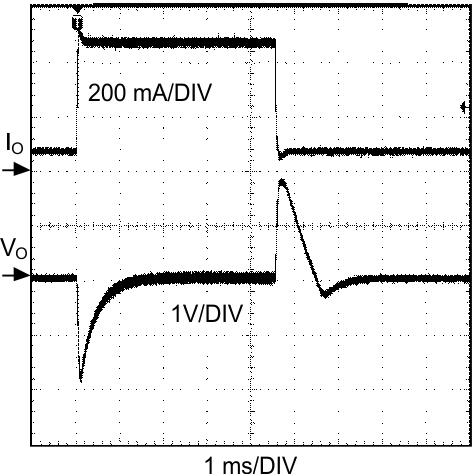
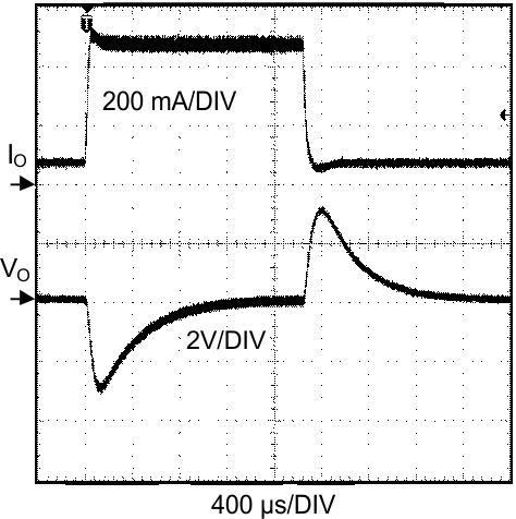
LM5022 Figure_21.gif
VIN = 16 V, IO = 50 mA to 0.5 A
Figure 28. Load Transient Response
LM5022 Figure_16.gif
VIN = 9 V, IO = 0.5 A
Figure 23. Switch Node Voltage
LM5022 Figure_18.gif
VIN = 9 V, IO = 0.5 A
Figure 25. Output Voltage Ripple AC Coupled
LM5022 Figure_20.gif
VIN = 9 V, IO = 50 mA to 0.5 A
Figure 27. Load Transient Response