ZHCSHC6I January 2007 – December 2017 LM5022
PRODUCTION DATA.
- 1 特性
- 2 应用
- 3 说明
- 4 修订历史记录
- 5 Pin Configuration and Functions
- 6 Specifications
- 7 Detailed Description
-
8 Application and Implementation
- 8.1 Application Information
- 8.2
Typical Application
- 8.2.1 Design Requirements
- 8.2.2
Detailed Design Procedure
- 8.2.2.1 Switching Frequency
- 8.2.2.2 MOSFET
- 8.2.2.3 Output Diode
- 8.2.2.4 Boost Inductor
- 8.2.2.5 Output Capacitor
- 8.2.2.6 VCC Decoupling Capacitor
- 8.2.2.7 Input Capacitor
- 8.2.2.8 Current Sense Filter
- 8.2.2.9 RSNS, RS2 and Current Limit
- 8.2.2.10 Control Loop Compensation
- 8.2.2.11 Efficiency Calculations
- 8.2.3 Application Curves
- 9 Power Supply Recommendations
- 10Layout
- 11器件和文档支持
- 12机械、封装和可订购信息
8.2.2.5 Output Capacitor
The output capacitor in a boost regulator supplies current to the load during the MOSFET on-time and also filters the AC portion of the load current during the off-time. This capacitor determines the steady-state output voltage ripple, ΔVO, a critical parameter for all voltage regulators. Output capacitors are selected based on their capacitance, CO, their equivalent series resistance (ESR) and their RMS or AC current rating.
The magnitude of ΔVO is comprised of three parts, and in steady-state the ripple voltage during the on-time is equal to the ripple voltage during the off-time. For simplicity the analysis is performed for the MOSFET turning off (off-time) only. The first part of the ripple voltage is the surge created as the output diode D1 turns on. At this point, inductor and diode current are at peak value, and the ripple voltage increase can be calculated with Equation 20.
The second portion of the ripple voltage is the increase due to the charging of CO through the output diode. This portion can be approximated with Equation 21.
The final portion of the ripple voltage is a decrease due to the flow of the diode and inductor current through the ESR of the output capacitor. This decrease can be calculated with Equation 22.
The total change in output voltage is Equation 23.
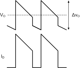
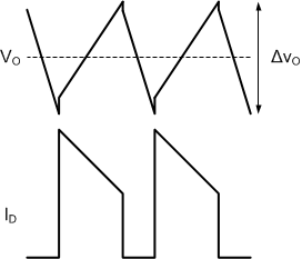
The combination of two positive terms and one negative term may yield an output voltage ripple with a net rise or a net fall during the converter off-time. The ESR of the output capacitor(s) has a strong influence on the slope and direction of ΔVO. Capacitors with high ESR such as tantalum and aluminum electrolytic create an output voltage ripple that is dominated by ΔVO1 and ΔVO3, with a shape shown in Figure 15. Ceramic capacitors, in contrast, have very low ESR and lower capacitance. The shape of the output ripple voltage is dominated by ΔVO2, with a shape shown in Figure 16.
 Figure 15. ΔVO Using High-ESR Capacitors
 Figure 16. ΔVO Using Low-ESR Capacitors
For this example the small size and high temperature rating of ceramic capacitors make them a good choice. The output ripple voltage waveform of Figure 16 is assumed, and the capacitance is selected first. The desired ΔVO is ±2% of 40 V, or 0.8 VP-P. Beginning with the calculation for ΔVO2, the required minimum capacitance is in Equation 24.
The next higher standard 20% capacitor value is 1 µF, however to provide margin for component tolerance and load transients two capacitors rated 4.7 µF each (CO= 9.4 µF) is used. Ceramic capacitors rated 4.7 µF ±20% are available from many manufacturers. The minimum quality dielectric that is suitable for switching power supply output capacitors is X5R, while X7R (or better) is preferred. Pay careful attention to the DC voltage rating and case size, as ceramic capacitors can lose 60% or more of their rated capacitance at the maximum DC voltage. This is the reason that ceramic capacitors are often de-rated to 50% of their capacitance at their working voltage. The output capacitors for this example has a 100-V rating in a 2220 case size.
The typical ESR of the selected capacitors is 3 mΩ each, and in parallel is approximately 1.5 mΩ. The worst-case value for ΔVO1 occurs during the peak current at minimum input voltage in Equation 25.
The worst-case capacitor charging ripple occurs at maximum duty cycle in Equation 26.
Finally, the worst-case value for ΔVO3 occurs when inductor ripple current is highest, at maximum input voltage in Equation 27.
The output voltage ripple can be estimated by summing the three terms in Equation 28.
The RMS current through the output capacitor(s) can be estimated using the following, worst-case equation in Equation 29.

The highest RMS current occurs at minimum input voltage. For this example the maximum output capacitor RMS current is calculated with Equation 30.
These 2220 case size devices are capable of sustaining RMS currents of over 3 A each, making them more than adequate for this application.