ZHCSHC6I January 2007 – December 2017 LM5022
PRODUCTION DATA.
- 1 特性
- 2 应用
- 3 说明
- 4 修订历史记录
- 5 Pin Configuration and Functions
- 6 Specifications
- 7 Detailed Description
-
8 Application and Implementation
- 8.1 Application Information
- 8.2
Typical Application
- 8.2.1 Design Requirements
- 8.2.2
Detailed Design Procedure
- 8.2.2.1 Switching Frequency
- 8.2.2.2 MOSFET
- 8.2.2.3 Output Diode
- 8.2.2.4 Boost Inductor
- 8.2.2.5 Output Capacitor
- 8.2.2.6 VCC Decoupling Capacitor
- 8.2.2.7 Input Capacitor
- 8.2.2.8 Current Sense Filter
- 8.2.2.9 RSNS, RS2 and Current Limit
- 8.2.2.10 Control Loop Compensation
- 8.2.2.11 Efficiency Calculations
- 8.2.3 Application Curves
- 9 Power Supply Recommendations
- 10Layout
- 11器件和文档支持
- 12机械、封装和可订购信息
8.2.2.10 Control Loop Compensation
The LM5022 uses peak current-mode PWM control to correct changes in output voltage due to line and load transients. Peak current-mode provides inherent cycle-by-cycle current limiting, improved line transient response, and easier control loop compensation.
The control loop is comprised of two parts. The first is the power stage, which consists of the pulse width modulator, output filter, and the load. The second part is the error amplifier, which is an op-amp configured as an inverting amplifier. Figure 17 shows the regulator control loop components.
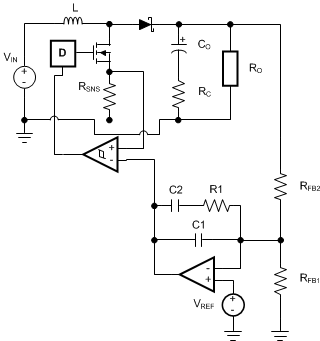 Figure 17. Power Stage and Error Amplifier
One popular method for selecting the compensation components is to create Bode plots of gain and phase for the power stage and error amplifier. Combined, they make the overall bandwidth and phase margin of the regulator easy to determine. Software tools such as Excel, MathCAD, and Matlab are useful for observing how changes in compensation or the power stage affect system gain and phase.
The power stage in a CCM peak current mode boost converter consists of the DC gain, APS, a single low-frequency pole, ƒLFP, the ESR zero, ƒZESR, a right-half plane zero, ƒRHP, and a double pole resulting from the sampling of the peak current. The power stage transfer function (also called the control-to-output transfer function) can be written with Equation 42, Equation 43, and Equation 44.
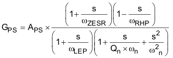
where
- the DC gain is defined as:

where
The system ESR zero is calculated with Equation 45.

The low-frequency pole is calculated with Equation 46.

The right-half plane zero is calculated with Equation 47.

The sampling double-pole quality factor is calculated with Equation 48.

The sampling double corner frequency is calculated with Equation 49.
The natural inductor current slope is calculated with Equation 50.
The external ramp slope is calculated with Equation 51.
In Equation 43, DC gain is highest when input voltage and output current are at the maximum. In this the example those conditions are VIN = 16 V and IO = 500 mA.
DC gain is 44 dB. The low-frequency pole fP = ωP/2π is at 423 Hz, the ESR zero fZ = ωZ/2π is at 5.6 MHz, and the right-half plane zero ƒRHP = ωRHP/2π is at 61 kHz. The sampling double-pole occurs at one-half of the switching frequency. Proper selection of slope compensation (through RS2) is most evident the sampling double pole. A well-selected RS2 value eliminates peaking in the gain and reduces the rate of change of the phase lag. Gain and phase plots for the power stage are shown in Figure 18 and Figure 19.
SPACE
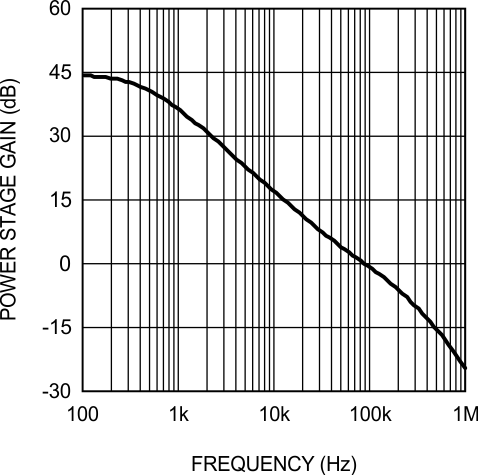 Figure 18. Power Stage Gain and Phase
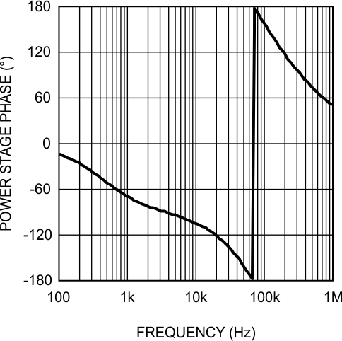 Figure 19. Power Stage Gain and Phase
The single pole causes a rolloff in the gain of –20 dB/decade at lower frequency. The combination of the RHP zero and sampling double pole maintain the slope out to beyond the switching frequency. The phase tends towards –90° at lower frequency but then increases to –180° and beyond from the RHP zero and the sampling double pole. The effect of the ESR zero is not seen because its frequency is several decades above the switching frequency. The combination of increasing gain and decreasing phase makes converters with RHP zeroes difficult to compensate. Setting the overall control loop bandwidth to 1/3 to 1/10 of the RHP zero frequency minimizes these negative effects, but requires a compromise in the control loop bandwidth. If this loop were left uncompensated, the bandwidth would be 89 kHz and the phase margin –54°. The converter would oscillate, and therefore is compensated using the error amplifier and a few passive components.
The transfer function of the compensation block (GEA) can be derived by treating the error amplifier as an inverting op-amp with input impedance ZI and feedback impedance ZF. The majority of applications require a Type II, or two-pole one-zero amplifier, shown in Figure 17. The LaPlace domain transfer function for this Type II network is given by Equation 52.

Many techniques exist for selecting the compensation component values. The following method is based upon setting the mid-band gain of the error amplifier transfer function first and then positioning the compensation zero and pole:
- Determine the desired control loop bandwidth: The control loop bandwidth (ƒ0dB) is the point at which the total control loop gain (H = GPS × GEA) is equal to 0 dB. For this example, a low bandwidth of 10 kHz, or approximately 1/6th of the RHP zero frequency, is chosen because of the wide variation in input voltage.
- Determine the gain of the power stage at ƒ0dB: This value, A, can be read graphically from the gain plot of GPS or calculated by replacing the ‘s’ terms in GPS with ‘2 πf0dB’. For this example, the gain at 10 kHz is approximately 16 dB.
- Calculate the negative of A and convert it to a linear gain: By setting the mid-band gain of the error amplifier to the negative of the power stage gain at f0dB, the control loop gain equals 0 dB at that frequency. For this example, –16 dB = 0.15 V/V.
- Select the resistance of the top feedback divider resistor RFB2: This value is arbitrary, however selecting a resistance between 10 kΩ and 100 kΩ leads to practical values of R1, C1, and C2. For this example, RFB2 = 20 kΩ 1%.
- Set Equation 55:
- Select a frequency for the compensation zero, ƒZ1: The suggested placement for this zero is at the low-frequency pole of the power stage, ƒLFP = ωLFP / 2π. For this example, ƒZ1 = ƒLFP = 423 Hz
- Set Equation 54.
- Select a frequency for the compensation pole, ƒP1: The suggested placement for this pole is at one-fifth of the switching frequency. For this example, ƒP1 = 100 kHz
- Set Equation 55.
- Plug the closest 1% tolerance values for RFB2 and R1, then the closest 10% values for C1 and C2 into GEA and model the error amp: The open-loop gain and bandwidth of the LM5022’s internal error amplifier are 75 dB and 4 MHz, respectively. Their effect on GEA can be modeled using Equation 56:
- Plot or evaluate the actual error amplifier transfer function:
- Plot or evaluate the complete control loop transfer function: The complete control loop transfer function is obtained by multiplying the power stage and error amplifier functions together. The bandwidth and phase margin can then be read graphically or evaluated numerically. The bandwidth of this example circuit at VIN = 16 V is 10.5 kHz with a phase margin of 66°.
- Re-evaluate at the corners of input voltage and output current: Boost converters exhibit significant change in their loop response when VIN and IO change. With the compensation fixed, the total control loop gain and phase must be checked to ensure a minimum phase margin of 45° over both line and load.
For this example: R1 = 0.15 × 20000 = 3 kΩ

For this example, C2 = 125 nF

For this example, C1 = 530 pF

ADC is a linear gain, the linear equivalent of 75 dB is approximately 5600 V/V. C1 = 560 pF 10%, C2 = 120 nF 10%, R1 = 3.01 kΩ 1%

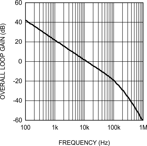 Figure 20. Overall Loop Gain and Phase
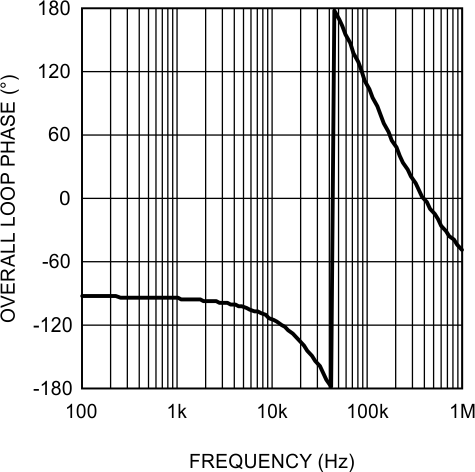 Figure 21. Overall Loop Gain and Phase